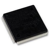
LFXP2-5E-5QN208C Lattice, LFXP2-5E-5QN208C Datasheet - Page 43

LFXP2-5E-5QN208C
Manufacturer Part Number
LFXP2-5E-5QN208C
Description
FPGA - Field Programmable Gate Array 5K LUTs 146I/O Inst- on DSP 1.2V -5 Spd
Manufacturer
Lattice
Datasheet
1.LFXP2-40E-5FN484I.pdf
(92 pages)
Specifications of LFXP2-5E-5QN208C
Number Of Macrocells
5000
Maximum Operating Frequency
200 MHz
Number Of Programmable I/os
146
Data Ram Size
10 KB
Supply Voltage (max)
1.14 V
Supply Current
17 mA
Maximum Operating Temperature
+ 85 C
Minimum Operating Temperature
0 C
Mounting Style
SMD/SMT
Supply Voltage (min)
1.26 V
Package / Case
PQFP-208
Lead Free Status / RoHS Status
Lead free / RoHS Compliant
Available stocks
Company
Part Number
Manufacturer
Quantity
Price
Company:
Part Number:
LFXP2-5E-5QN208C
Manufacturer:
Lattice Semiconductor Corporation
Quantity:
10 000
Part Number:
LFXP2-5E-5QN208C
Manufacturer:
LATTICE
Quantity:
20 000
Lattice Semiconductor
For more information on device configuration, please see TN1141,
Soft Error Detect (SED) Support
LatticeXP2 devices have dedicated logic to perform Cyclic Redundancy Code (CRC) checks. During configuration,
the configuration data bitstream can be checked with the CRC logic block. In addition, LatticeXP2 devices can be
programmed for checking soft errors in SRAM. The SED operation can run in the background during user mode
(normal operation). In the event a soft error occurs, the device can be programmed to either reload from a known
good boot image (from internal Flash or external SPI memory) or generate an error signal.
For further information on SED support, please see TN1130,
On-Chip Oscillator
Every LatticeXP2 device has an internal CMOS oscillator that is used to derive a Master Clock (CCLK) for configu-
ration. The oscillator and CCLK run continuously and are available to user logic after configuration is complete. The
available CCLK frequencies are listed in Table 2-14. When a different CCLK frequency is selected during the
design process, the following sequence takes place:
1. Device powers up with the default CCLK frequency.
2. During configuration, users select a different CCLK frequency.
3. CCLK frequency changes to the selected frequency after clock configuration bits are received.
This internal CMOS oscillator is available to the user by routing it as an input clock to the clock tree. For further
information on the use of this oscillator for configuration or user mode, please see TN1141,
FIG Usage
Table 2-14. Selectable CCLKs and Oscillator Frequencies During Configuration and User Mode
original backup configuration and try again. This all can be done without power cycling the system. For more
information please see TN1220,
Guide.
LatticeXP2 Dual Boot
1. Software default oscillator frequency.
2. Software default CCLK frequency.
3. Frequency not valid for CCLK.
CCLK/Oscillator (MHz)
2-40
163
2.5
3.1
80
4.3
5.4
6.9
8.1
9.2
10
13
15
20
26
32
40
54
3
1
2
3
Feature.
LatticeXP2 Soft Error Detection (SED) Usage
LatticeXP2 sysCONFIG Usage
LatticeXP2 Family Data Sheet
LatticeXP2 sysCON-
Architecture
Guide.
Guide.


