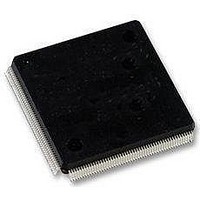
LFXP2-5E-5QN208C Lattice, LFXP2-5E-5QN208C Datasheet - Page 26

LFXP2-5E-5QN208C
Manufacturer Part Number
LFXP2-5E-5QN208C
Description
FPGA - Field Programmable Gate Array 5K LUTs 146I/O Inst- on DSP 1.2V -5 Spd
Manufacturer
Lattice
Datasheet
1.LFXP2-40E-5FN484I.pdf
(92 pages)
Specifications of LFXP2-5E-5QN208C
Number Of Macrocells
5000
Maximum Operating Frequency
200 MHz
Number Of Programmable I/os
146
Data Ram Size
10 KB
Supply Voltage (max)
1.14 V
Supply Current
17 mA
Maximum Operating Temperature
+ 85 C
Minimum Operating Temperature
0 C
Mounting Style
SMD/SMT
Supply Voltage (min)
1.26 V
Package / Case
PQFP-208
Lead Free Status / RoHS Status
Lead free / RoHS Compliant
Available stocks
Company
Part Number
Manufacturer
Quantity
Price
Company:
Part Number:
LFXP2-5E-5QN208C
Manufacturer:
Lattice Semiconductor Corporation
Quantity:
10 000
Part Number:
LFXP2-5E-5QN208C
Manufacturer:
LATTICE
Quantity:
20 000
Lattice Semiconductor
MULTADDSUBSUM sysDSP Element
In this case, the operands A0 and B0 are multiplied and the result is added/subtracted with the result of the multi-
plier operation of operands A1 and B1. Additionally the operands A2 and B2 are multiplied and the result is added/
subtracted with the result of the multiplier operation of operands A3 and B3. The result of both addition/subtraction
are added in a summation block. The user can enable the input, output and pipeline registers. Figure 2-23 shows
the MULTADDSUBSUM sysDSP element.
Figure 2-23. MULTADDSUBSUM
Clock, Clock Enable and Reset Resources
Global Clock, Clock Enable (CE) and Reset (RST) signals from routing are available to every DSP block. From four
clock sources (CLK0, CLK1, CLK2, CLK3) one clock is selected for each input register, pipeline register and output
Multiplicand A0
Multiplicand A1
Multiplicand A2
Multiplicand A3
Multiplier B0
Multiplier B1
Multiplier B2
Multiplier B3
Signed A
Signed B
Shift Register B Out
Addn0
Addn1
Shift Register B In
n
n
n
n
Register B
Register B
Register B
Register B
Input Data
Input Data
Input Data
Input Data
n
n
n
n
n
n
n
n
n
Register
Register
Register
Register
Input
Input
Input
Input
m
m
m
m
Input Data
Register A
Input Data
Register A
Input Data
Register A
Input Data
Register A
m
m
m
m
m
Shift Register A Out
Shift Register A In
m
m
m
m
Register
Register
Register
Register
Pipeline
Pipeline
Pipeline
Pipeline
m
n
n
n
m
n
m
n
2-23
Multiplier
Multiplier
Multiplier
Multiplier
To Add/Sub1
To Add/Sub0, Add/Sub1
To Add/Sub0, Add/Sub1
To Add/Sub0
Pipeline
Register
Pipeline
Register
x
x
x
x
Register
Register
Pipeline
Pipeline
(default)
(default)
m+n
m+n
(default)
(default)
m+n
m+n
Add/Sub0
Add/Sub1
CLK (CLK0,CLK1,CLK2,CLK3)
CE (CE0,CE1,CE2,CE3)
RST(RST0,RST1,RST2,RST3)
LatticeXP2 Family Data Sheet
m+n+1
m+n+1
SUM
m+n+2
m+n+2
Architecture
Output


