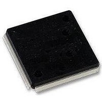
LFXP2-5E-5QN208C Lattice, LFXP2-5E-5QN208C Datasheet - Page 31

LFXP2-5E-5QN208C
Manufacturer Part Number
LFXP2-5E-5QN208C
Description
FPGA - Field Programmable Gate Array 5K LUTs 146I/O Inst- on DSP 1.2V -5 Spd
Manufacturer
Lattice
Datasheet
1.LFXP2-40E-5FN484I.pdf
(92 pages)
Specifications of LFXP2-5E-5QN208C
Number Of Macrocells
5000
Maximum Operating Frequency
200 MHz
Number Of Programmable I/os
146
Data Ram Size
10 KB
Supply Voltage (max)
1.14 V
Supply Current
17 mA
Maximum Operating Temperature
+ 85 C
Minimum Operating Temperature
0 C
Mounting Style
SMD/SMT
Supply Voltage (min)
1.26 V
Package / Case
PQFP-208
Lead Free Status / RoHS Status
Lead free / RoHS Compliant
Available stocks
Company
Part Number
Manufacturer
Quantity
Price
Company:
Part Number:
LFXP2-5E-5QN208C
Manufacturer:
Lattice Semiconductor Corporation
Quantity:
10 000
Part Number:
LFXP2-5E-5QN208C
Manufacturer:
LATTICE
Quantity:
20 000
Lattice Semiconductor
The signal DDRCLKPOL controls the polarity of the clock used in the synchronization registers. It ensures ade-
quate timing when data is transferred from the DQS to system clock domain. For further discussion on this topic,
see the DDR Memory section of this data sheet.
Figure 2-26. Input Register Block
Output Register Block
The output register block provides the ability to register signals from the core of the device before they are passed
to the sysIO buffers. The blocks on the PIOs on the left, right and bottom contain registers for SDR operation that
are combined with an additional latch for DDR operation. Figure 2-27 shows the diagram of the Output Register
Block for PIOs.
In SDR mode, ONEG0 feeds one of the flip-flops that then feeds the output. The flip-flop can be configured as a D-
type or latch. In DDR mode, ONEG0 and OPOS0 are fed into registers on the positive edge of the clock. At the next
clock cycle the registered OPOS0 is latched. A multiplexer running off the same clock cycle selects the correct reg-
ister to feed the output (D0).
By combining output blocks of the complementary PIOs and sharing some registers from input blocks, a gearbox
function can be implemented, to take four data streams ONEG0A, ONEG1A, ONEG1B and ONEG1B. Figure 2-27
CLK0 (of PIO B)
CLK0 (of PIO A)
DDRCLKPOL
DDRCLKPOL
(From sysIO
(From sysIO
Routing
Routing
DEL [3:0]
From
From
Buffer)
Buffer)
DEL [3:0]
Delayed
Delayed
DI
DI
DQS
DQS
CLKA
CLKB
1. Shared with output register
2. Selected PIO.
True PIO (A) in LVDS I/O Pair
Comp PIO (B) in LVDS I/O Pair
Dynamic Delay
Dynamic Delay
Fixed Delay
Fixed Delay
0
1
0
1
0
1
0
1
DDR Registers
DDR Registers
D
D
D
D
D-Type
D-Type
D-Type
D-Type
Q
Q
Q
Q
D1
D1
0
1
D
D
D-Type
DDRSRC
D-Type
D0
0
1
Q
Q
2-28
Gearbox Configuration Bit
D2
D0
D2
0
1
0
1
SDR & Sync
SDR & Sync
Registers
Registers
D
D
D
D
/LATCH
/LATCH
/LATCH
/LATCH
D-Type
D-Type
D-Type
D-Type
Q
Q
Q
Q
Note: Simplified version does not
show CE and SET/RESET details
LatticeXP2 Family Data Sheet
Clock Transfer Registers
Clock Transfer Registers
D
D
D
D
D-Type
D-Type
D-Type
D-Type
Q
Q
Q
Q
1
1
1
1
INCK
To DQS Delay Block
INDD
IPOS0A
QPOS0A
IPOS1A
QPOS1A
INCK
To DQS Delay Block
INDD
IPOS0B
QPOS0B
IPOS1B
QPOS1B
Architecture
Routing
Routing
To
To
2
2
2
2


