LFXP2-5E-5QN208C Lattice, LFXP2-5E-5QN208C Datasheet - Page 7
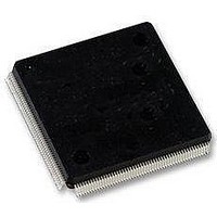
LFXP2-5E-5QN208C
Manufacturer Part Number
LFXP2-5E-5QN208C
Description
FPGA - Field Programmable Gate Array 5K LUTs 146I/O Inst- on DSP 1.2V -5 Spd
Manufacturer
Lattice
Datasheet
1.LFXP2-40E-5FN484I.pdf
(92 pages)
Specifications of LFXP2-5E-5QN208C
Number Of Macrocells
5000
Maximum Operating Frequency
200 MHz
Number Of Programmable I/os
146
Data Ram Size
10 KB
Supply Voltage (max)
1.14 V
Supply Current
17 mA
Maximum Operating Temperature
+ 85 C
Minimum Operating Temperature
0 C
Mounting Style
SMD/SMT
Supply Voltage (min)
1.26 V
Package / Case
PQFP-208
Lead Free Status / RoHS Status
Lead free / RoHS Compliant
Available stocks
Company
Part Number
Manufacturer
Quantity
Price
Company:

Part Number:
LFXP2-5E-5QN208C
Manufacturer:
Lattice Semiconductor Corporation
Quantity:
10 000
Part Number:
LFXP2-5E-5QN208C
Manufacturer:
LATTICE
Quantity:
20 000


Lattice Semiconductor
Figure 2-3. Slice Diagram
Table 2-2. Slice Signal Descriptions
1. See Figure 2-3 for connection details.
2. Requires two PFUs.
Function
Output
Output
Output
Output
Output
Input
Input
Input
Input
Input
Input
Input
Input
Input
Input
Routing
From
Inter-PFU signal
Inter-slice signal
Inter-slice signal
Inter-PFU signal
Multi-purpose
Multi-purpose
Control signal
Control signal
Control signal
Data signals
Data signals
Data signals
Data signals
Data signal
Data signal
FXB
FXA
CLK
LSR
Type
M1
M0
CE
A1
B1
C1
D1
A0
B0
C0
D0
* Not in Slice 3
For Slices 0 and 2, memory control signals are generated from Slice 1 as follows:
WCK is CLK
WRE is from LSR
DI[3:2] for Slice 2 and DI[1:0] for Slice 0 data
WAD [A:D] is a 4bit address from slice 1 LUT input
FCO from Slice/PFU, FCI into Different Slice/PFU
A0, B0, C0, D0
A1, B1, C1, D1
Signal Names
Q0, Q1
F0, F1
OFX0
OFX1
FCO
LSR
CLK
FXA
FXB
FCI
M0
M1
CE
FCI into Slice/PFU, FCO from Different Slice/PFU
LUT4 &
CARRY*
LUT4 &
CARRY*
Inputs to LUT4
Inputs to LUT4
Multipurpose Input
Multipurpose Input
Clock Enable
Local Set/Reset
System Clock
Fast Carry-In
Intermediate signal to generate LUT6 and LUT7
Intermediate signal to generate LUT6 and LUT7
LUT4 output register bypass signals
Register outputs
Output of a LUT5 MUX
Output of a LUT6, LUT7, LUT8
Slice 2 of each PFU is the fast carry chain output
CO
CO
CI
CI
2-4
F/SUM
F/SUM
1
LUT5
Mux
Description
LatticeXP2 Family Data Sheet
2
MUX depending on the slice
SLICE
D
D
FF*
FF*
Routing
OFX1
F1
Q1
To
OFX0
F0
Q0
1
Architecture
Related parts for LFXP2-5E-5QN208C
Image
Part Number
Description
Manufacturer
Datasheet
Request
R

Part Number:
Description:
FPGA - Field Programmable Gate Array 5K LUTs 172I/O Inst- on DSP 1.2V -5 Spd
Manufacturer:
Lattice
Datasheet:

Part Number:
Description:
FPGA - Field Programmable Gate Array 5K LUTs 172 I/O Inst on DSP 1.2V -5 Spd
Manufacturer:
Lattice
Datasheet:

Part Number:
Description:
FPGA - Field Programmable Gate Array 5K LUTs 100 I/O Inst on DSP 1.2V -5 Spd
Manufacturer:
Lattice
Datasheet:

Part Number:
Description:
FPGA - Field Programmable Gate Array 5K LUTs 100I/O Inst- on DSP 1.2V -5 Spd
Manufacturer:
Lattice
Datasheet:

Part Number:
Description:
FPGA LatticeXP2 Family 5000 Cells Flash Technology 1.2V 256-Pin FTBGA
Manufacturer:
LATTICE SEMICONDUCTOR
Datasheet:
Part Number:
Description:
FPGA LatticeXP2 Family 5000 Cells Flash Technology 1.2V 256-Pin FTBGA
Manufacturer:
LATTICE SEMICONDUCTOR
Datasheet:
Part Number:
Description:
IC DSP 5KLUTS 100I/O 144TQFP
Manufacturer:
Lattice
Datasheet:
Part Number:
Description:
IC DSP 5KLUTS 86I/O 132CSBGA
Manufacturer:
Lattice
Datasheet:
Part Number:
Description:
IC DSP 5KLUTS 86I/O 132CSBGA
Manufacturer:
Lattice
Datasheet:
Part Number:
Description:
IC DSP 5KLUTS 146I/O 208PQFP
Manufacturer:
Lattice
Datasheet:
Part Number:
Description:
IC DSP 5KLUTS 146I/O 208PQFP
Manufacturer:
Lattice
Datasheet:
Part Number:
Description:
IC DSP 5KLUTS 172I/O 256FTBGA
Manufacturer:
Lattice
Datasheet:
Part Number:
Description:
IC FPGA 5KLUTS 86I/O 132-BGA
Manufacturer:
Lattice
Datasheet:
Part Number:
Description:
IC FPGA 5KLUTS 86I/O 132-BGA
Manufacturer:
Lattice
Datasheet:
Part Number:
Description:
IC FPGA 5KLUTS 86I/O 132-BGA
Manufacturer:
Lattice
Datasheet: