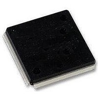
LFXP2-5E-5QN208C Lattice, LFXP2-5E-5QN208C Datasheet - Page 40

LFXP2-5E-5QN208C
Manufacturer Part Number
LFXP2-5E-5QN208C
Description
FPGA - Field Programmable Gate Array 5K LUTs 146I/O Inst- on DSP 1.2V -5 Spd
Manufacturer
Lattice
Datasheet
1.LFXP2-40E-5FN484I.pdf
(92 pages)
Specifications of LFXP2-5E-5QN208C
Number Of Macrocells
5000
Maximum Operating Frequency
200 MHz
Number Of Programmable I/os
146
Data Ram Size
10 KB
Supply Voltage (max)
1.14 V
Supply Current
17 mA
Maximum Operating Temperature
+ 85 C
Minimum Operating Temperature
0 C
Mounting Style
SMD/SMT
Supply Voltage (min)
1.26 V
Package / Case
PQFP-208
Lead Free Status / RoHS Status
Lead free / RoHS Compliant
Available stocks
Company
Part Number
Manufacturer
Quantity
Price
Company:
Part Number:
LFXP2-5E-5QN208C
Manufacturer:
Lattice Semiconductor Corporation
Quantity:
10 000
Part Number:
LFXP2-5E-5QN208C
Manufacturer:
LATTICE
Quantity:
20 000
Lattice Semiconductor
Table 2-13. Supported Output Standards
Hot Socketing
LatticeXP2 devices have been carefully designed to ensure predictable behavior during power-up and power-
down. Power supplies can be sequenced in any order. During power-up and power-down sequences, the I/Os
remain in tri-state until the power supply voltage is high enough to ensure reliable operation. In addition, leakage
into I/O pins is controlled to within specified limits. This allows for easy integration with the rest of the system.
These capabilities make the LatticeXP2 ideal for many multiple power supply and hot-swap applications.
IEEE 1149.1-Compliant Boundary Scan Testability
All LatticeXP2 devices have boundary scan cells that are accessed through an IEEE 1149.1 compliant Test Access
Port (TAP). This allows functional testing of the circuit board, on which the device is mounted, through a serial scan
path that can access all critical logic nodes. Internal registers are linked internally, allowing test data to be shifted in
Single-ended Interfaces
LVTTL
LVCMOS33
LVCMOS25
LVCMOS18
LVCMOS15
LVCMOS12
LVCMOS33, Open Drain
LVCMOS25, Open Drain
LVCMOS18, Open Drain
LVCMOS15, Open Drain
LVCMOS12, Open Drain
PCI33
HSTL18 Class I, II
HSTL15 Class I
SSTL33 Class I, II
SSTL25 Class I, II
SSTL18 Class I, II
Differential Interfaces
Differential SSTL33, Class I, II
Differential SSTL25, Class I, II
Differential SSTL18, Class I, II
Differential HSTL18, Class I, II
Differential HSTL15, Class I
LVDS
MLVDS
BLVDS
LVPECL
RSDS
LVCMOS33D
1. Emulated with external resistors.
2. On the left and right edges, LVDS outputs are supported with a dedicated differential output driver on 50% of the I/Os. This
solution does not require external resistors at the driver.
1, 2
1
1
1
1
Output Standard
1
4mA, 8mA, 12mA, 16mA, 20mA
4mA, 8mA, 12mA, 16mA, 20mA
4mA, 8mA, 12mA, 16mA, 20mA
4mA, 8mA, 12mA 16mA, 20mA
4mA, 8mA, 12mA 16mA, 20mA
4mA, 8mA, 12mA 16mA, 20mA
4mA, 8mA, 12mA, 16mA
4mA, 8mA, 12mA 16mA
4mA, 8mA
2mA, 6mA
4mA, 8mA
2mA, 6mA
2-37
Drive
N/A
N/A
N/A
N/A
N/A
N/A
N/A
N/A
N/A
N/A
N/A
N/A
N/A
N/A
N/A
N/A
LatticeXP2 Family Data Sheet
V
CCIO
3.3
3.3
2.5
1.5
1.2
3.3
1.8
1.5
3.3
2.5
3.3
2.5
1.8
1.8
1.5
2.5
2.5
2.5
3.3
2.5
3.3
1.8
—
—
—
—
—
1.8
(Nom.)
Architecture


