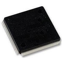
LFXP2-5E-5QN208C Lattice, LFXP2-5E-5QN208C Datasheet - Page 79

LFXP2-5E-5QN208C
Manufacturer Part Number
LFXP2-5E-5QN208C
Description
FPGA - Field Programmable Gate Array 5K LUTs 146I/O Inst- on DSP 1.2V -5 Spd
Manufacturer
Lattice
Datasheet
1.LFXP2-40E-5FN484I.pdf
(92 pages)
Specifications of LFXP2-5E-5QN208C
Number Of Macrocells
5000
Maximum Operating Frequency
200 MHz
Number Of Programmable I/os
146
Data Ram Size
10 KB
Supply Voltage (max)
1.14 V
Supply Current
17 mA
Maximum Operating Temperature
+ 85 C
Minimum Operating Temperature
0 C
Mounting Style
SMD/SMT
Supply Voltage (min)
1.26 V
Package / Case
PQFP-208
Lead Free Status / RoHS Status
Lead free / RoHS Compliant
Available stocks
Company
Part Number
Manufacturer
Quantity
Price
Company:
Part Number:
LFXP2-5E-5QN208C
Manufacturer:
Lattice Semiconductor Corporation
Quantity:
10 000
Part Number:
LFXP2-5E-5QN208C
Manufacturer:
LATTICE
Quantity:
20 000
Lattice Semiconductor
Signal Descriptions (Cont.)
TDO
VCCJ
Configuration Pads (Used during sysCONFIG)
CFG[1:0]
INITN
PROGRAMN
DONE
CCLK
SISPI
SOSPI
CSSPIN
CSSPISN
TOE
1. If not actively driven, the internal pull-up may not be sufficient. An external pull-up resistor of 4.7k to 10k
2. When using the device in Master SPI mode, it must be mutually exclusive from JTAG operations (i.e. TCK tied to GND) or the JTAG TCK
must be free-running when used in a system JTAG test environment. If Master SPI mode is used in conjunction with a JTAG download
cable, the device power cycle is required after the cable is unplugged.
1
2
2
2
Signal Name
I/O
I/O
I/O
I/O
I/O
I/O
—
O
O
I
I
I
I
Output pin. Test Data Out pin used to shift data out of a device using 1149.1.
Power supply pin for JTAG Test Access Port.
Mode pins used to specify configuration mode values latched on rising edge
of INITN. During configuration, an internal pull-up is enabled.
Open Drain pin. Indicates the FPGA is ready to be configured. During config-
uration, a pull-up is enabled.
Initiates configuration sequence when asserted low. This pin always has an
active pull-up.
Open Drain pin. Indicates that the configuration sequence is complete, and
the startup sequence is in progress.
Configuration Clock for configuring an FPGA in sysCONFIG mode.
Input data pin in slave SPI mode and Output data pin in Master SPI mode.
Output data pin in slave SPI mode and Input data pin in Master SPI mode.
Chip select for external SPI Flash memory in Master SPI mode. This pin has
a weak internal pull-up.
Chip select in Slave SPI mode. This pin has a weak internal pull-up.
Test Output Enable tristates all I/O pins when driven low. This pin has a weak
internal pull-up, but when not used an external pull-up to V
mended.
4-2
Description
LatticeXP2 Family Data Sheet
is recommended.
Pinout Information
CC
is recom-


