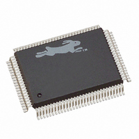
20-668-0003 Rabbit Semiconductor, 20-668-0003 Datasheet - Page 64

20-668-0003
Manufacturer Part Number
20-668-0003
Description
IC CPU RABBIT2000 30MHZ 100PQFP
Manufacturer
Rabbit Semiconductor
Datasheet
1.20-668-0003.pdf
(228 pages)
Specifications of 20-668-0003
Processor Type
Rabbit 2000 8-Bit
Speed
30MHz
Voltage
2.7V, 3V, 3.3V, 5V
Mounting Type
Surface Mount
Package / Case
100-MQFP, 100-PQFP
Data Bus Width
8 bit
Maximum Clock Frequency
30 MHz
Operating Supply Voltage
0 V to 5.5 V
Maximum Operating Temperature
+ 85 C
Mounting Style
SMD/SMT
Minimum Operating Temperature
- 40 C
Number Of Programmable I/os
40
Number Of Timers
8 & 10 bit
Lead Free Status / RoHS Status
Lead free / RoHS Compliant
Features
-
Lead Free Status / Rohs Status
Lead free / RoHS Compliant
Other names
20-668-0003
316-1062
316-1062
Available stocks
Company
Part Number
Manufacturer
Quantity
Price
Company:
Part Number:
20-668-0003
Manufacturer:
Rabbit Semiconductor
Quantity:
10 000
- Current page: 64 of 228
- Download datasheet (2Mb)
5.4 Bus Timing
The external bus has essentially the same timing for memory cycles or I/O cycles. A
memory cycle begins with the chip select and the address lines. One clock later, the out-
put enable is asserted for a read. The output data and the write enable are asserted for a
write.
In some cases, the timing shown in Figure 5-4 may be prefixed by a false memory access
during the first clock, which is followed by the access sequence shown in Figure 5-4. In
this case, the address and often the chip select will change values after one clock and
assume the final values for the memory to be actually accessed. Output enable and write
enable are always delayed by one clock from the time the final, stable address and chip
select are enabled. Normally the false memory access attempts to start another instruction
access cycle, which is aborted after one clock when the processor realizes that a read data
or write data bus cycle is needed. The user should not attempt a design that uses the chip
select or a memory address as a clock or state changing signal without taking this into con-
sideration.
58
Notes:
Read may have no wait states.
Write cycles and I/O read cycles have at least 1 wait state. Clock
may be asymmetric if clock doubler used. I/O chip select avail-
able on port E as option.
T1
Tw
Figure 5-4. Bus Timing Read and Write
T2
valid
Address (20 for memory, 16 for I/O)
Data for write 3-s drive starts at end of T1
/OEn or /IORD and /BUFEN (/BUFEN rd or wr)
Data for read
/WEn or /IOWR
/IOCSn or /CSn
Rabbit 2000 Microprocessor User’s Manual
Related parts for 20-668-0003
Image
Part Number
Description
Manufacturer
Datasheet
Request
R

Part Number:
Description:
IC CPU RABBIT4000 128-LQFP
Manufacturer:
Rabbit Semiconductor
Datasheet:

Part Number:
Description:
IC MPU RABIT3000A 55.5MHZ128LQFP
Manufacturer:
Rabbit Semiconductor
Datasheet:

Part Number:
Description:
Microprocessors - MPU Rabbit 3000 TFBGA Microprocessor
Manufacturer:
Rabbit Semiconductor

Part Number:
Description:
Microprocessors - MPU Rabbit 4000 LQFP Microprocessor
Manufacturer:
Rabbit Semiconductor

Part Number:
Description:
IC, I/O EXPANDER, 8BIT, 40MHZ, TQFP-64
Manufacturer:
Rabbit Semiconductor

Part Number:
Description:
SCRs 1.5A 200uA 400V Sensing
Manufacturer:
Littelfuse Inc
Datasheet:

Part Number:
Description:
CARD 6-RELAY SMARTSTAR SR9500
Manufacturer:
Rabbit Semiconductor
Datasheet:

Part Number:
Description:
WIRE-BOARD CONN RECEPTACLE, 6POS, 3.96MM
Manufacturer:
TE Connectivity
Datasheet:

Part Number:
Description:
ADAPTER 20 PIN .420" PLUGS(6PCS)
Manufacturer:
Logical Systems Inc.
Datasheet:

Part Number:
Description:
CONN BARRIER BLOCK .438" 20 POS
Manufacturer:
Cinch Connectors
Datasheet:

Part Number:
Description:
20 MODII 2PC HDR DR SHRD, ROHS
Manufacturer:
TE Connectivity
Datasheet:

Part Number:
Description:
WIRE-BOARD CONN RECEPTACLE, 6POS, 3.96MM
Manufacturer:
TE Connectivity
Datasheet:


