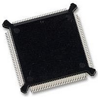
MC68332GCEH20 Freescale Semiconductor, MC68332GCEH20 Datasheet - Page 222

MC68332GCEH20
Manufacturer Part Number
MC68332GCEH20
Description
IC MCU 32BIT 20MHZ 132-PQFP
Manufacturer
Freescale Semiconductor
Series
M683xxr
Specifications of MC68332GCEH20
Core Processor
CPU32
Core Size
32-Bit
Speed
20MHz
Connectivity
EBI/EMI, SCI, SPI, UART/USART
Peripherals
POR, PWM, WDT
Number Of I /o
15
Program Memory Type
ROMless
Ram Size
2K x 8
Voltage - Supply (vcc/vdd)
4.5 V ~ 5.5 V
Oscillator Type
Internal
Operating Temperature
-40°C ~ 85°C
Package / Case
132-QFP
Controller Family/series
68K
No. Of I/o's
15
Ram Memory Size
2KB
Cpu Speed
20MHz
No. Of Timers
1
Embedded Interface Type
QSPI, SCI, UART
Digital Ic Case Style
PQFP
Rohs Compliant
Yes
Data Bus Width
32 bit
Data Ram Size
2 KB
Interface Type
QSPI, SCI, UART
Maximum Clock Frequency
20 MHz
Number Of Programmable I/os
15
Number Of Timers
16
Maximum Operating Temperature
+ 85 C
Mounting Style
SMD/SMT
Minimum Operating Temperature
- 40 C
Lead Free Status / RoHS Status
Lead free / RoHS Compliant
Eeprom Size
-
Program Memory Size
-
Data Converters
-
Lead Free Status / Rohs Status
Details
Available stocks
Company
Part Number
Manufacturer
Quantity
Price
Company:
Part Number:
MC68332GCEH20
Manufacturer:
Freescale Semiconductor
Quantity:
10 000
Part Number:
MC68332GCEH20
Manufacturer:
FREESCALE
Quantity:
20 000
- Current page: 222 of 265
- Download datasheet (7Mb)
D.2.6 PORTE0/PORTE1 — Port E Data Register
D.2.7 DDRE — Port E Data Direction Register
D.2.8 PEPAR — Port E Pin Assignment Register
D-8
15
15
15
PORTE is an internal data latch that can be accessed at two locations. PORTE can be
read or written at any time. If a pin in I/O port E is configured as an output, the corre-
sponding bit value is driven out on the pin. When a pin is configured for output, a read
of PORTE returns the latched bit value; when a pin is configured for input, a read re-
turns the pin logic level.
Bits in this register control the direction of the port E pin drivers when pins are config-
ured for I/O. Setting a bit configures the corresponding pin as an output; clearing a bit
configures the corresponding pin as an input. This register can be read or written at
any time.
Bits in this register determine the function of port E pins. Setting a bit assigns the cor-
responding pin to a bus control signal; clearing a bit assigns the pin to I/O port E.
RESET:
RESET:
RESET:
PEPAR Bit
PEPA7
PEPA6
PEPA5
PEPA4
PEPA3
PEPA2
PEPA1
PEPA0
NOT USED
NOT USED
NOT USED
Freescale Semiconductor, Inc.
For More Information On This Product,
Go to: www.freescale.com
REGISTER SUMMARY
Port E Pin Assignments
Port E Signal
8
8
8
PE7
PE6
PE5
PE4
PE3
PE2
PE1
PE0
PEPA7 PEPA6 PEPA5 PEPA4 PEPA3 PEPA2 PEPA1 PEPA0
DATA8 DATA8 DATA8 DATA8 DATA8 DATA8 DATA8 DATA8
DDE7
PE7
7
U
7
0
7
DDE6
PE6
U
6
6
0
6
DDE5
PE5
U
5
5
0
5
DDE4
PE4
U
4
4
0
4
Bus Control Signal
$YFFA11, $YFFA13
DDE3
PE3
DSACK1
DSACK0
U
3
3
0
3
AVEC
RMC
SIZ1
SIZ0
DS
AS
DDE2
USER’S MANUAL
PE2
U
2
2
0
2
$YFFA15
$YFFA17
DDE1
PE1
U
1
1
0
1
MC68332
DDE0
PE0
0
U
0
0
0
Related parts for MC68332GCEH20
Image
Part Number
Description
Manufacturer
Datasheet
Request
R
Part Number:
Description:
Manufacturer:
Freescale Semiconductor, Inc
Datasheet:
Part Number:
Description:
Manufacturer:
Freescale Semiconductor, Inc
Datasheet:
Part Number:
Description:
Manufacturer:
Freescale Semiconductor, Inc
Datasheet:
Part Number:
Description:
Manufacturer:
Freescale Semiconductor, Inc
Datasheet:
Part Number:
Description:
Manufacturer:
Freescale Semiconductor, Inc
Datasheet:
Part Number:
Description:
Manufacturer:
Freescale Semiconductor, Inc
Datasheet:
Part Number:
Description:
Manufacturer:
Freescale Semiconductor, Inc
Datasheet:
Part Number:
Description:
Manufacturer:
Freescale Semiconductor, Inc
Datasheet:
Part Number:
Description:
Manufacturer:
Freescale Semiconductor, Inc
Datasheet:
Part Number:
Description:
Manufacturer:
Freescale Semiconductor, Inc
Datasheet:
Part Number:
Description:
Manufacturer:
Freescale Semiconductor, Inc
Datasheet:
Part Number:
Description:
Manufacturer:
Freescale Semiconductor, Inc
Datasheet:
Part Number:
Description:
Manufacturer:
Freescale Semiconductor, Inc
Datasheet:
Part Number:
Description:
Manufacturer:
Freescale Semiconductor, Inc
Datasheet:
Part Number:
Description:
Manufacturer:
Freescale Semiconductor, Inc
Datasheet:


