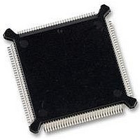
MC68332GCEH20 Freescale Semiconductor, MC68332GCEH20 Datasheet - Page 63

MC68332GCEH20
Manufacturer Part Number
MC68332GCEH20
Description
IC MCU 32BIT 20MHZ 132-PQFP
Manufacturer
Freescale Semiconductor
Series
M683xxr
Specifications of MC68332GCEH20
Core Processor
CPU32
Core Size
32-Bit
Speed
20MHz
Connectivity
EBI/EMI, SCI, SPI, UART/USART
Peripherals
POR, PWM, WDT
Number Of I /o
15
Program Memory Type
ROMless
Ram Size
2K x 8
Voltage - Supply (vcc/vdd)
4.5 V ~ 5.5 V
Oscillator Type
Internal
Operating Temperature
-40°C ~ 85°C
Package / Case
132-QFP
Controller Family/series
68K
No. Of I/o's
15
Ram Memory Size
2KB
Cpu Speed
20MHz
No. Of Timers
1
Embedded Interface Type
QSPI, SCI, UART
Digital Ic Case Style
PQFP
Rohs Compliant
Yes
Data Bus Width
32 bit
Data Ram Size
2 KB
Interface Type
QSPI, SCI, UART
Maximum Clock Frequency
20 MHz
Number Of Programmable I/os
15
Number Of Timers
16
Maximum Operating Temperature
+ 85 C
Mounting Style
SMD/SMT
Minimum Operating Temperature
- 40 C
Lead Free Status / RoHS Status
Lead free / RoHS Compliant
Eeprom Size
-
Program Memory Size
-
Data Converters
-
Lead Free Status / Rohs Status
Details
Available stocks
Company
Part Number
Manufacturer
Quantity
Price
Company:
Part Number:
MC68332GCEH20
Manufacturer:
Freescale Semiconductor
Quantity:
10 000
Part Number:
MC68332GCEH20
Manufacturer:
FREESCALE
Quantity:
20 000
- Current page: 63 of 265
- Download datasheet (7Mb)
4.5.1 Synchronization to CLKOUT
4.5.2 Regular Bus Cycles
MC68332
USER’S MANUAL
Fast-termination cycles, which are two-cycle external accesses with no wait states,
use chip-select logic to generate handshaking signals internally. Chip-select logic can
also be used to insert wait states before internal generation of handshaking signals.
Refer to 4.5.3 Fast Termination Cycles and 4.8 Chip Selects for more information.
Bus control signal timing, as well as chip-select signal timing, are specified in APPEN-
DIX A ELECTRICAL CHARACTERISTICS. Refer to the SIM Reference Manual (SIM-
RM/AD) for more information about each type of bus cycle.
The MCU is responsible for de-skewing signals it issues at both the start and the end
of a cycle. In addition, the MCU is responsible for de-skewing acknowledge and data
signals from peripheral devices.
External devices connected to the MCU bus can operate at a clock frequency different
from the frequencies of the MCU as long as the external devices satisfy the interface
signal timing constraints. Although bus cycles are classified as asynchronous, they are
interpreted relative to the MCU system clock output (CLKOUT).
Descriptions are made in terms of individual system clock states, labeled {S0, S1,
S2,..., SN}. The designation “state” refers to the logic level of the clock signal, and
does not correspond to any implemented machine state. A clock cycle consists of two
successive states. Refer to APPENDIX A ELECTRICAL CHARACTERISTICS for
more information.
Bus cycles terminated by DSACK assertion normally require a minimum of three CLK-
OUT cycles. To support systems that use CLKOUT to generate DSACK and other in-
puts, asynchronous input setup time and asynchronous input hold times are specified.
When these specifications are met, the MCU is guaranteed to recognize the appropri-
ate signal on a specific edge of the CLKOUT signal.
For a read cycle, when assertion of DSACK is recognized on a particular falling edge
of the clock, valid data is latched into the MCU on the next falling clock edge, provided
that the data meets the data setup time. In this case, the parameter for asynchronous
operation can be ignored.
When a system asserts DSACK for the required window around the falling edge of S2
and obeys the bus protocol by maintaining DSACK and BERR or HALT until and
throughout the clock edge that negates AS, no wait states are inserted. The bus cycle
runs at the maximum speed of three clocks per cycle.
To ensure proper operation in a system synchronized to CLKOUT, when either BERR,
or BERR and HALT is asserted after DSACK, BERR (or BERR and HALT) assertion
must satisfy the appropriate data-in setup and hold times before the falling edge of the
clock cycle after DSACK is recognized.
The following paragraphs contain a discussion of cycles that use external bus control
logic. Refer to 4.5.3 Fast Termination Cycles for information about fast cycles.
Freescale Semiconductor, Inc.
For More Information On This Product,
SYSTEM INTEGRATION MODULE
Go to: www.freescale.com
4-23
Related parts for MC68332GCEH20
Image
Part Number
Description
Manufacturer
Datasheet
Request
R
Part Number:
Description:
Manufacturer:
Freescale Semiconductor, Inc
Datasheet:
Part Number:
Description:
Manufacturer:
Freescale Semiconductor, Inc
Datasheet:
Part Number:
Description:
Manufacturer:
Freescale Semiconductor, Inc
Datasheet:
Part Number:
Description:
Manufacturer:
Freescale Semiconductor, Inc
Datasheet:
Part Number:
Description:
Manufacturer:
Freescale Semiconductor, Inc
Datasheet:
Part Number:
Description:
Manufacturer:
Freescale Semiconductor, Inc
Datasheet:
Part Number:
Description:
Manufacturer:
Freescale Semiconductor, Inc
Datasheet:
Part Number:
Description:
Manufacturer:
Freescale Semiconductor, Inc
Datasheet:
Part Number:
Description:
Manufacturer:
Freescale Semiconductor, Inc
Datasheet:
Part Number:
Description:
Manufacturer:
Freescale Semiconductor, Inc
Datasheet:
Part Number:
Description:
Manufacturer:
Freescale Semiconductor, Inc
Datasheet:
Part Number:
Description:
Manufacturer:
Freescale Semiconductor, Inc
Datasheet:
Part Number:
Description:
Manufacturer:
Freescale Semiconductor, Inc
Datasheet:
Part Number:
Description:
Manufacturer:
Freescale Semiconductor, Inc
Datasheet:
Part Number:
Description:
Manufacturer:
Freescale Semiconductor, Inc
Datasheet:


