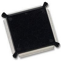
MC68332GCEH20 Freescale Semiconductor, MC68332GCEH20 Datasheet - Page 65

MC68332GCEH20
Manufacturer Part Number
MC68332GCEH20
Description
IC MCU 32BIT 20MHZ 132-PQFP
Manufacturer
Freescale Semiconductor
Series
M683xxr
Specifications of MC68332GCEH20
Core Processor
CPU32
Core Size
32-Bit
Speed
20MHz
Connectivity
EBI/EMI, SCI, SPI, UART/USART
Peripherals
POR, PWM, WDT
Number Of I /o
15
Program Memory Type
ROMless
Ram Size
2K x 8
Voltage - Supply (vcc/vdd)
4.5 V ~ 5.5 V
Oscillator Type
Internal
Operating Temperature
-40°C ~ 85°C
Package / Case
132-QFP
Controller Family/series
68K
No. Of I/o's
15
Ram Memory Size
2KB
Cpu Speed
20MHz
No. Of Timers
1
Embedded Interface Type
QSPI, SCI, UART
Digital Ic Case Style
PQFP
Rohs Compliant
Yes
Data Bus Width
32 bit
Data Ram Size
2 KB
Interface Type
QSPI, SCI, UART
Maximum Clock Frequency
20 MHz
Number Of Programmable I/os
15
Number Of Timers
16
Maximum Operating Temperature
+ 85 C
Mounting Style
SMD/SMT
Minimum Operating Temperature
- 40 C
Lead Free Status / RoHS Status
Lead free / RoHS Compliant
Eeprom Size
-
Program Memory Size
-
Data Converters
-
Lead Free Status / Rohs Status
Details
Available stocks
Company
Part Number
Manufacturer
Quantity
Price
Company:
Part Number:
MC68332GCEH20
Manufacturer:
Freescale Semiconductor
Quantity:
10 000
Part Number:
MC68332GCEH20
Manufacturer:
FREESCALE
Quantity:
20 000
- Current page: 65 of 265
- Download datasheet (7Mb)
4.5.2.2 Write Cycle
MC68332
USER’S MANUAL
During a write cycle, the MCU transfers data to an external memory or peripheral de-
vice. If the instruction specifies a long-word or word operation, the MCU attempts to
write two bytes at once. For a byte operation, the MCU writes one byte. The portion of
the data bus upon which each byte is written depends on operand size, peripheral ad-
dress, and peripheral port size.
Refer to 4.4.2 Dynamic Bus Sizing and 4.4.4 Misaligned Operands for more infor-
mation. Figure 4-10 is a flowchart of a write-cycle operation for a word transfer. Refer
to the SIM Reference Manual (SIMRM/AD) for more information.
2) DRIVE ADDRESS ON ADDR[23:0]
3) DRIVE FUNCTION CODE ON FC[2:0]
4) DRIVE SIZ[1:0] FOR OPERAND SIZE
1) SET R/W TO READ
NEGATE AS AND DS (S5)
START NEXT CYCLE (S0)
ASSERT AS AND DS (S1)
ADDRESS DEVICE (S0)
DECODE DSACK (S3)
LATCH DATA (S4)
MCU
Figure 4-9 Word Read Cycle Flowchart
Freescale Semiconductor, Inc.
For More Information On This Product,
SYSTEM INTEGRATION MODULE
Go to: www.freescale.com
1) DECODE ADDR, R/W, SIZ[1:0], DS
2) PLACE DATA ON DATA[15:0] OR
3) DRIVE DSACK SIGNALS
1) REMOVE DATA FROM DATA BUS
2) NEGATE DSACK
DATA[15:8] IF 8-BIT DATA
TERMINATE CYCLE (S5)
PRESENT DATA (S2)
PERIPHERAL
RD CYC FLOW
4-25
Related parts for MC68332GCEH20
Image
Part Number
Description
Manufacturer
Datasheet
Request
R
Part Number:
Description:
Manufacturer:
Freescale Semiconductor, Inc
Datasheet:
Part Number:
Description:
Manufacturer:
Freescale Semiconductor, Inc
Datasheet:
Part Number:
Description:
Manufacturer:
Freescale Semiconductor, Inc
Datasheet:
Part Number:
Description:
Manufacturer:
Freescale Semiconductor, Inc
Datasheet:
Part Number:
Description:
Manufacturer:
Freescale Semiconductor, Inc
Datasheet:
Part Number:
Description:
Manufacturer:
Freescale Semiconductor, Inc
Datasheet:
Part Number:
Description:
Manufacturer:
Freescale Semiconductor, Inc
Datasheet:
Part Number:
Description:
Manufacturer:
Freescale Semiconductor, Inc
Datasheet:
Part Number:
Description:
Manufacturer:
Freescale Semiconductor, Inc
Datasheet:
Part Number:
Description:
Manufacturer:
Freescale Semiconductor, Inc
Datasheet:
Part Number:
Description:
Manufacturer:
Freescale Semiconductor, Inc
Datasheet:
Part Number:
Description:
Manufacturer:
Freescale Semiconductor, Inc
Datasheet:
Part Number:
Description:
Manufacturer:
Freescale Semiconductor, Inc
Datasheet:
Part Number:
Description:
Manufacturer:
Freescale Semiconductor, Inc
Datasheet:
Part Number:
Description:
Manufacturer:
Freescale Semiconductor, Inc
Datasheet:


