MC68332GCEH20 Freescale Semiconductor, MC68332GCEH20 Datasheet - Page 71
MC68332GCEH20
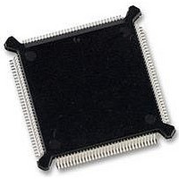
Manufacturer Part Number
MC68332GCEH20
Description
IC MCU 32BIT 20MHZ 132-PQFP
Manufacturer
Freescale Semiconductor
Series
M683xxr
Specifications of MC68332GCEH20
Core Processor
CPU32
Core Size
32-Bit
Speed
20MHz
Connectivity
EBI/EMI, SCI, SPI, UART/USART
Peripherals
POR, PWM, WDT
Number Of I /o
15
Program Memory Type
ROMless
Ram Size
2K x 8
Voltage - Supply (vcc/vdd)
4.5 V ~ 5.5 V
Oscillator Type
Internal
Operating Temperature
-40°C ~ 85°C
Package / Case
132-QFP
Controller Family/series
68K
No. Of I/o's
15
Ram Memory Size
2KB
Cpu Speed
20MHz
No. Of Timers
1
Embedded Interface Type
QSPI, SCI, UART
Digital Ic Case Style
PQFP
Rohs Compliant
Yes
Data Bus Width
32 bit
Data Ram Size
2 KB
Interface Type
QSPI, SCI, UART
Maximum Clock Frequency
20 MHz
Number Of Programmable I/os
15
Number Of Timers
16
Maximum Operating Temperature
+ 85 C
Mounting Style
SMD/SMT
Minimum Operating Temperature
- 40 C
Lead Free Status / RoHS Status
Lead free / RoHS Compliant
Eeprom Size
-
Program Memory Size
-
Data Converters
-
Lead Free Status / Rohs Status
Details
Available stocks
Company
Part Number
Manufacturer
Quantity
Price
Company:

Part Number:
MC68332GCEH20
Manufacturer:
Freescale Semiconductor
Quantity:
10 000
Part Number:
MC68332GCEH20
Manufacturer:
FREESCALE
Quantity:
20 000


4.5.4.2 LPSTOP Broadcast Cycle
4.5.5 Bus Exception Control Cycles
MC68332
USER’S MANUAL
15
0
Low-power stop is initiated by the CPU32. Individual modules can be stopped by set-
ting the STOP bits in each module configuration register, or the SIM can turn off sys-
tem clocks after execution of the LPSTOP instruction. When the CPU executes
LPSTOP, the LPSTOP broadcast cycle is generated. The SIM brings the MCU out of
low-power mode when either an interrupt of higher priority than the stored mask or a
reset occurs. Refer to and SECTION 5 CENTRAL PROCESSING UNIT for more in-
formation.
During an LPSTOP broadcast cycle, the CPU performs a CPU space write to address
$3FFFE. This write puts a copy of the interrupt mask value in the clock control logic.
The mask is encoded on the data bus as shown in Figure 4-13. The LPSTOP CPU
space cycle is shown externally (if the bus is available) as an indication to external de-
vices that the MCU is going into low-power stop mode. The SIM provides an internally
generated DSACK response to this cycle. The timing of this bus cycle is the same as
for a fast write cycle.
An external device or a chip-select circuit must assert at least one of the DSACK[1:0]
signals or the AVEC signal to terminate a bus cycle normally. Bus error processing oc-
curs when bus cycles are not terminated in the expected manner. The internal bus
monitor can be used to generate BERR internally, causing a bus error exception to be
taken. Bus cycles can also be terminated by assertion of the external BERR or HALT
signal, or by assertion of the two signals simultaneously.
Acceptable bus cycle termination sequences are summarized as follows. The case
numbers refer to Table 4-5, which indicates the results of each type of bus cycle ter-
mination.
Normal Termination
Halt Termination
Bus Error Termination
DSACK is asserted; BERR and HALT remain negated (case 1).
HALT is asserted at the same time or before DSACK, and BERR remains negated
(case 2).
BERR is asserted in lieu of, at the same time as, or before DSACK, or after
DSACK, and HALT remains negated; BERR is negated at the same time or after
DSACK.
14
0
13
0
12
0
Figure 4-13 LPSTOP Interrupt Mask Level
Freescale Semiconductor, Inc.
11
For More Information On This Product,
0
SYSTEM INTEGRATION MODULE
10
0
Go to: www.freescale.com
9
0
8
0
7
0
6
0
5
0
4
0
3
0
2
IP MASK
1
4-31
0
Related parts for MC68332GCEH20
Image
Part Number
Description
Manufacturer
Datasheet
Request
R

Part Number:
Description:
Manufacturer:
Freescale Semiconductor, Inc
Datasheet:
Part Number:
Description:
Manufacturer:
Freescale Semiconductor, Inc
Datasheet:
Part Number:
Description:
Manufacturer:
Freescale Semiconductor, Inc
Datasheet:
Part Number:
Description:
Manufacturer:
Freescale Semiconductor, Inc
Datasheet:
Part Number:
Description:
Manufacturer:
Freescale Semiconductor, Inc
Datasheet:
Part Number:
Description:
Manufacturer:
Freescale Semiconductor, Inc
Datasheet:
Part Number:
Description:
Manufacturer:
Freescale Semiconductor, Inc
Datasheet:
Part Number:
Description:
Manufacturer:
Freescale Semiconductor, Inc
Datasheet:
Part Number:
Description:
Manufacturer:
Freescale Semiconductor, Inc
Datasheet:
Part Number:
Description:
Manufacturer:
Freescale Semiconductor, Inc
Datasheet:
Part Number:
Description:
Manufacturer:
Freescale Semiconductor, Inc
Datasheet:
Part Number:
Description:
Manufacturer:
Freescale Semiconductor, Inc
Datasheet:
Part Number:
Description:
Manufacturer:
Freescale Semiconductor, Inc
Datasheet:
Part Number:
Description:
Manufacturer:
Freescale Semiconductor, Inc
Datasheet:
Part Number:
Description:
Manufacturer:
Freescale Semiconductor, Inc
Datasheet: