MC68332GCEH20 Freescale Semiconductor, MC68332GCEH20 Datasheet - Page 243
MC68332GCEH20
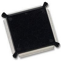
Manufacturer Part Number
MC68332GCEH20
Description
IC MCU 32BIT 20MHZ 132-PQFP
Manufacturer
Freescale Semiconductor
Series
M683xxr
Specifications of MC68332GCEH20
Core Processor
CPU32
Core Size
32-Bit
Speed
20MHz
Connectivity
EBI/EMI, SCI, SPI, UART/USART
Peripherals
POR, PWM, WDT
Number Of I /o
15
Program Memory Type
ROMless
Ram Size
2K x 8
Voltage - Supply (vcc/vdd)
4.5 V ~ 5.5 V
Oscillator Type
Internal
Operating Temperature
-40°C ~ 85°C
Package / Case
132-QFP
Controller Family/series
68K
No. Of I/o's
15
Ram Memory Size
2KB
Cpu Speed
20MHz
No. Of Timers
1
Embedded Interface Type
QSPI, SCI, UART
Digital Ic Case Style
PQFP
Rohs Compliant
Yes
Data Bus Width
32 bit
Data Ram Size
2 KB
Interface Type
QSPI, SCI, UART
Maximum Clock Frequency
20 MHz
Number Of Programmable I/os
15
Number Of Timers
16
Maximum Operating Temperature
+ 85 C
Mounting Style
SMD/SMT
Minimum Operating Temperature
- 40 C
Lead Free Status / RoHS Status
Lead free / RoHS Compliant
Eeprom Size
-
Program Memory Size
-
Data Converters
-
Lead Free Status / Rohs Status
Details
Available stocks
Company
Part Number
Manufacturer
Quantity
Price
Company:

Part Number:
MC68332GCEH20
Manufacturer:
Freescale Semiconductor
Quantity:
10 000
Part Number:
MC68332GCEH20
Manufacturer:
FREESCALE
Quantity:
20 000


D.4.16 CR[0:F] — Command RAM
PCS[3:0] — Peripheral Chip Select
CONT — Continue
BITSE — Bits per Transfer Enable
DT — Delay after Transfer
DSCK — PCS to SCK Delay
MC68332
USER’S MANUAL
Command RAM is used by the QSPI when in master mode. The CPU32 writes one
byte of control information to this segment for each QSPI command to be executed.
The QSPI cannot modify information in command RAM.
Command RAM consists of 16 bytes. Each byte is divided into two fields. The periph-
eral chip-select field enables peripherals for transfer. The command control field pro-
vides transfer options.
A maximum of 16 commands can be in the queue. Queue execution proceeds from
the address in NEWQP through the address in ENDQP (both of these fields are in
SPCR2).
Peripheral chip-select bits are used to select an external device for serial data transfer.
More than one peripheral chip select may be activated at a time, and more than one
peripheral chip can be connected to each PCS pin, provided proper fanout is ob-
served. PCS0 shares a pin with the slave select (SS) signal, which initiates slave mode
serial transfer. If SS is taken low when the QSPI is in master mode, a mode fault oc-
curs.
The QSPI provides a variable delay at the end of serial transfer to facilitate interfacing
with peripherals that have a latency requirement. The delay between transfers is de-
termined by the SPCR1 DTL field.
0 = Control of chip selects returned to PORTQS after transfer is complete.
1 = Peripheral chip selects remain asserted after transfer is complete.
0 = Eight bits
1 = Number of bits set in BITS field of SPCR0
0 = PCS valid to SCK transition is one-half SCK.
1 = SPCR1 DSCKL field specifies delay from PCS valid to SCK.
*The PCS0 bit represents the dual-function PCS0/SS.
CONT
CONT
—
7
COMMAND CONTROL
BITSE
BITSE
—
6
Freescale Semiconductor, Inc.
For More Information On This Product,
DT
DT
—
5
Go to: www.freescale.com
REGISTER SUMMARY
DSCK
DSCK
—
4
PCS3
PCS3
—
3
PERIPHERAL CHIP SELECT
PCS2
PCS2
—
2
PCS1
PCS1
—
1
$YFFD40–$YFFD4F
PCS0*
PCS0*
—
0
D-29
Related parts for MC68332GCEH20
Image
Part Number
Description
Manufacturer
Datasheet
Request
R

Part Number:
Description:
Manufacturer:
Freescale Semiconductor, Inc
Datasheet:
Part Number:
Description:
Manufacturer:
Freescale Semiconductor, Inc
Datasheet:
Part Number:
Description:
Manufacturer:
Freescale Semiconductor, Inc
Datasheet:
Part Number:
Description:
Manufacturer:
Freescale Semiconductor, Inc
Datasheet:
Part Number:
Description:
Manufacturer:
Freescale Semiconductor, Inc
Datasheet:
Part Number:
Description:
Manufacturer:
Freescale Semiconductor, Inc
Datasheet:
Part Number:
Description:
Manufacturer:
Freescale Semiconductor, Inc
Datasheet:
Part Number:
Description:
Manufacturer:
Freescale Semiconductor, Inc
Datasheet:
Part Number:
Description:
Manufacturer:
Freescale Semiconductor, Inc
Datasheet:
Part Number:
Description:
Manufacturer:
Freescale Semiconductor, Inc
Datasheet:
Part Number:
Description:
Manufacturer:
Freescale Semiconductor, Inc
Datasheet:
Part Number:
Description:
Manufacturer:
Freescale Semiconductor, Inc
Datasheet:
Part Number:
Description:
Manufacturer:
Freescale Semiconductor, Inc
Datasheet:
Part Number:
Description:
Manufacturer:
Freescale Semiconductor, Inc
Datasheet:
Part Number:
Description:
Manufacturer:
Freescale Semiconductor, Inc
Datasheet: