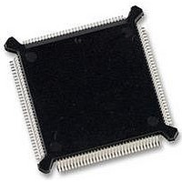
MC68332GCEH20 Freescale Semiconductor, MC68332GCEH20 Datasheet - Page 51

MC68332GCEH20
Manufacturer Part Number
MC68332GCEH20
Description
IC MCU 32BIT 20MHZ 132-PQFP
Manufacturer
Freescale Semiconductor
Series
M683xxr
Specifications of MC68332GCEH20
Core Processor
CPU32
Core Size
32-Bit
Speed
20MHz
Connectivity
EBI/EMI, SCI, SPI, UART/USART
Peripherals
POR, PWM, WDT
Number Of I /o
15
Program Memory Type
ROMless
Ram Size
2K x 8
Voltage - Supply (vcc/vdd)
4.5 V ~ 5.5 V
Oscillator Type
Internal
Operating Temperature
-40°C ~ 85°C
Package / Case
132-QFP
Controller Family/series
68K
No. Of I/o's
15
Ram Memory Size
2KB
Cpu Speed
20MHz
No. Of Timers
1
Embedded Interface Type
QSPI, SCI, UART
Digital Ic Case Style
PQFP
Rohs Compliant
Yes
Data Bus Width
32 bit
Data Ram Size
2 KB
Interface Type
QSPI, SCI, UART
Maximum Clock Frequency
20 MHz
Number Of Programmable I/os
15
Number Of Timers
16
Maximum Operating Temperature
+ 85 C
Mounting Style
SMD/SMT
Minimum Operating Temperature
- 40 C
Lead Free Status / RoHS Status
Lead free / RoHS Compliant
Eeprom Size
-
Program Memory Size
-
Data Converters
-
Lead Free Status / Rohs Status
Details
Available stocks
Company
Part Number
Manufacturer
Quantity
Price
Company:
Part Number:
MC68332GCEH20
Manufacturer:
Freescale Semiconductor
Quantity:
10 000
Part Number:
MC68332GCEH20
Manufacturer:
FREESCALE
Quantity:
20 000
- Current page: 51 of 265
- Download datasheet (7Mb)
MC68332
USER’S MANUAL
1. Maintain low-leakage on the XFC node. See Appendix A electrical characteristics for more information.
2. Recommended loop filter for reduced sensitivity to low-frequency noise.
ply must be used as the V
be placed as close as possible to the V
cy. When an external system clock signal is applied and the PLL is disabled, V
should be connected to the V
AD) for more information regarding system clock power supply conditioning.
A voltage controlled oscillator (VCO) generates the system clock signal. To maintain
a 50% clock duty cycle, VCO frequency is either two or four times system clock fre-
quency, depending on the state of the X bit in SYNCR. A portion of the clock signal is
fed back to a divider/counter. The divider controls the frequency of one input to a
phase comparator. The other phase comparator input is a reference signal, either from
the crystal oscillator or from an external source. The comparator generates a control
signal proportional to the difference in phase between the two inputs. The signal is low-
pass filtered and used to correct VCO output frequency.
Filter geometry can vary, depending upon the external environment and required clock
stability. Figure 4-6 shows two recommended filters. XFC pin leakage must be as
specified in APPENDIX A ELECTRICAL CHARACTERISTICS to maintain optimum
stability and PLL performance.
An external filter network connected to the XFC pin is not required when an external
system clock signal is applied and the PLL is disabled. The XFC pin must be left float-
ing in this case.
The synthesizer locks when VCO frequency is equal to EXTAL frequency. Lock time
is affected by the filter time constant and by the amount of difference between the two
comparator inputs. Whenever comparator input changes, the synthesizer must relock.
Lock status is shown by the SLOCK bit in SYNCR. During power-up, the MCU does
not come out of reset state until the synthesizer locks. Crystal type, characteristic fre-
quency, and layout of external oscillator circuitry affect lock time.
V
SSI
0.01 F
0.1 F
C3
C4
NORMAL OPERATING
ENVIRONMENT
Figure 4-6 System Clock Filter Networks
Freescale Semiconductor, Inc.
0.1 F
For More Information On This Product,
C1
DDSYN
SYSTEM INTEGRATION MODULE
DD
Go to: www.freescale.com
XFC
V
DDSYN
supply. Refer to the SIM Reference Manual (SIMRM/
1
source. Adequate external bypass capacitors should
DDSYN
pin to assure stable operating frequen-
V
SSI
0.01 F
0.1 F
C3
C4
HIGH-STABILITY OPERATING
ENVIRONMENT
0.1 F
C1
0.01 F
C2
18k
R1
XFC
V
DDSYN
1, 2
16/32 XFC CONN
DDSYN
4-11
Related parts for MC68332GCEH20
Image
Part Number
Description
Manufacturer
Datasheet
Request
R
Part Number:
Description:
Manufacturer:
Freescale Semiconductor, Inc
Datasheet:
Part Number:
Description:
Manufacturer:
Freescale Semiconductor, Inc
Datasheet:
Part Number:
Description:
Manufacturer:
Freescale Semiconductor, Inc
Datasheet:
Part Number:
Description:
Manufacturer:
Freescale Semiconductor, Inc
Datasheet:
Part Number:
Description:
Manufacturer:
Freescale Semiconductor, Inc
Datasheet:
Part Number:
Description:
Manufacturer:
Freescale Semiconductor, Inc
Datasheet:
Part Number:
Description:
Manufacturer:
Freescale Semiconductor, Inc
Datasheet:
Part Number:
Description:
Manufacturer:
Freescale Semiconductor, Inc
Datasheet:
Part Number:
Description:
Manufacturer:
Freescale Semiconductor, Inc
Datasheet:
Part Number:
Description:
Manufacturer:
Freescale Semiconductor, Inc
Datasheet:
Part Number:
Description:
Manufacturer:
Freescale Semiconductor, Inc
Datasheet:
Part Number:
Description:
Manufacturer:
Freescale Semiconductor, Inc
Datasheet:
Part Number:
Description:
Manufacturer:
Freescale Semiconductor, Inc
Datasheet:
Part Number:
Description:
Manufacturer:
Freescale Semiconductor, Inc
Datasheet:
Part Number:
Description:
Manufacturer:
Freescale Semiconductor, Inc
Datasheet:


