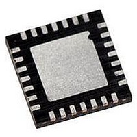
PIC16LF723A-I/ML Microchip Technology, PIC16LF723A-I/ML Datasheet - Page 107

PIC16LF723A-I/ML
Manufacturer Part Number
PIC16LF723A-I/ML
Description
MCU PIC 3.5K FLASH XLP 28-QFN
Manufacturer
Microchip Technology
Series
PIC® XLP™ 16Fr
Specifications of PIC16LF723A-I/ML
Core Size
8-Bit
Program Memory Size
7KB (4K x 14)
Peripherals
Brown-out Detect/Reset, POR, PWM, WDT
Core Processor
PIC
Speed
20MHz
Connectivity
I²C, SPI, UART/USART
Number Of I /o
25
Program Memory Type
FLASH
Ram Size
192 x 8
Voltage - Supply (vcc/vdd)
1.8 V ~ 3.6 V
Data Converters
A/D 11x8b
Oscillator Type
Internal
Operating Temperature
-40°C ~ 85°C
Package / Case
28-VQFN Exposed Pad, 28-HVQFN, 28-SQFN, 28-DHVQFN
Controller Family/series
PIC16LF
No. Of I/o's
25
Ram Memory Size
192Byte
Cpu Speed
20MHz
No. Of Timers
3
Lead Free Status / RoHS Status
Lead free / RoHS Compliant
Eeprom Size
-
Lead Free Status / RoHS Status
Lead free / RoHS Compliant, Lead free / RoHS Compliant
- Current page: 107 of 284
- Download datasheet (3Mb)
TABLE 12-5:
12.6.3
When Timer1 Gate Toggle mode is enabled, it is pos-
sible to measure the full-cycle length of a Timer1 gate
signal, as opposed to the duration of a single level
pulse.
The Timer1 gate source is routed through a flip-flop that
changes state on every incrementing edge of the sig-
nal. See Figure 12-4 for timing details.
Timer1 Gate Toggle mode is enabled by setting the
T1GTM bit of the T1GCON register. When the T1GTM
bit is cleared, the flip-flop is cleared and held clear. This
is necessary in order to control which edge is
measured.
2010 Microchip Technology Inc.
Note:
WDTE
1
1
0
0
TIMER1 GATE TOGGLE MODE
Enabling Toggle mode at the same time
as changing the gate polarity may result in
indeterminate operation.
WDT/TIMER1 GATE INTERACTION
TMR1GE = 1
T1GSS = 11
and
N
Y
Y
N
WDT Oscillator
Enable
N
Y
Y
Y
PIC16F/LF722A/723A
WDT Reset
12.6.4
When Timer1 Gate Single-Pulse mode is enabled, it is
possible to capture a single pulse gate event. Timer1
Gate Single-Pulse mode is first enabled by setting the
T1GSPM bit in the T1GCON register. Next, the
T1GGO/DONE bit in the T1GCON register must be set.
The Timer1 will be fully enabled on the next
incrementing edge. On the next trailing edge of the
pulse, the T1GGO/DONE bit will automatically be
cleared. No other gate events will be allowed to
increment Timer1 until the T1GGO/DONE bit is once
again set in software.
Clearing the T1GSPM bit of the T1GCON register will
also clear the T1GGO/DONE bit. See Figure 12-5 for
timing details.
Enabling the Toggle mode and the Single-Pulse mode
simultaneously will permit both sections to work
together. This allows the cycle times on the Timer1 gate
source to be measured. See Figure 12-6 for timing
details.
12.6.5
When Timer1 gate value status is utilized, it is possible
to read the most current level of the gate control value.
The value is stored in the T1GVAL bit in the T1GCON
register. The T1GVAL bit is valid even when the Timer1
gate is not enabled (TMR1GE bit is cleared).
12.6.6
When Timer1 gate event interrupt is enabled, it is pos-
sible to generate an interrupt upon the completion of a
gate event. When the falling edge of T1GVAL occurs,
the TMR1GIF flag bit in the PIR1 register will be set. If
the TMR1GIE bit in the PIE1 register is set, then an
interrupt will be recognized.
The TMR1GIF flag bit operates even when the Timer1
gate is not enabled (TMR1GE bit is cleared).
N
N
Y
Y
TIMER1 GATE SINGLE-PULSE
MODE
TIMER1 GATE VALUE STATUS
TIMER1 GATE EVENT INTERRUPT
Wake-up
N
N
Y
Y
WDT Available for
DS41417A-page 107
T1G Source
N
N
Y
Y
Related parts for PIC16LF723A-I/ML
Image
Part Number
Description
Manufacturer
Datasheet
Request
R

Part Number:
Description:
IC PIC MCU FLASH 8KX14 28-SPDIP
Manufacturer:
Microchip Technology
Datasheet:

Part Number:
Description:
IC PIC MCU FLASH 8KX14 28-QFN
Manufacturer:
Microchip Technology
Datasheet:

Part Number:
Description:
IC PIC MCU FLASH 8KX14 28-SPDIP
Manufacturer:
Microchip Technology
Datasheet:

Part Number:
Description:
IC PIC MCU FLASH 8KX14 28-QFN
Manufacturer:
Microchip Technology
Datasheet:

Part Number:
Description:
IC PIC MCU FLASH 8KX14 28-SOIC
Manufacturer:
Microchip Technology
Datasheet:

Part Number:
Description:
IC PIC MCU FLASH 8KX14 28-SSOP
Manufacturer:
Microchip Technology
Datasheet:

Part Number:
Description:
IC PIC MCU FLASH 8KX14 28-SSOP
Manufacturer:
Microchip Technology
Datasheet:

Part Number:
Description:
7 KB Flash, 16 MHz Int. Osc, NanoWatt XLP 28 SOIC .300in TUBE
Manufacturer:
Microchip Technology
Datasheet:

Part Number:
Description:
IC PIC MCU FLASH 2KX14 28SOIC
Manufacturer:
Microchip Technology
Datasheet:

Part Number:
Description:
IC PIC MCU FLASH 2KX14 28QFN
Manufacturer:
Microchip Technology
Datasheet:

Part Number:
Description:
IC PIC MCU FLASH 2KX14 28DIP
Manufacturer:
Microchip Technology
Datasheet:

Part Number:
Description:
IC MCU FLASH 2KX14 28SOIC
Manufacturer:
Microchip Technology

Part Number:
Description:
IC PIC MCU FLASH 2KX14 28QFN
Manufacturer:
Microchip Technology

Part Number:
Description:
IC PIC MCU FLASH 2KX14 28SSOP
Manufacturer:
Microchip Technology
Datasheet:

Part Number:
Description:
IC, 8BIT MCU, PIC16LF, 32MHZ, QFN-28
Manufacturer:
Microchip Technology
Datasheet:


