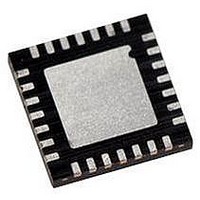
PIC16LF723A-I/ML Microchip Technology, PIC16LF723A-I/ML Datasheet - Page 16

PIC16LF723A-I/ML
Manufacturer Part Number
PIC16LF723A-I/ML
Description
MCU PIC 3.5K FLASH XLP 28-QFN
Manufacturer
Microchip Technology
Series
PIC® XLP™ 16Fr
Specifications of PIC16LF723A-I/ML
Core Size
8-Bit
Program Memory Size
7KB (4K x 14)
Peripherals
Brown-out Detect/Reset, POR, PWM, WDT
Core Processor
PIC
Speed
20MHz
Connectivity
I²C, SPI, UART/USART
Number Of I /o
25
Program Memory Type
FLASH
Ram Size
192 x 8
Voltage - Supply (vcc/vdd)
1.8 V ~ 3.6 V
Data Converters
A/D 11x8b
Oscillator Type
Internal
Operating Temperature
-40°C ~ 85°C
Package / Case
28-VQFN Exposed Pad, 28-HVQFN, 28-SQFN, 28-DHVQFN
Controller Family/series
PIC16LF
No. Of I/o's
25
Ram Memory Size
192Byte
Cpu Speed
20MHz
No. Of Timers
3
Lead Free Status / RoHS Status
Lead free / RoHS Compliant
Eeprom Size
-
Lead Free Status / RoHS Status
Lead free / RoHS Compliant, Lead free / RoHS Compliant
- Current page: 16 of 284
- Download datasheet (3Mb)
PIC16F/LF722A/723A
2.2
The data memory is partitioned into multiple banks
which contain the General Purpose Registers (GPRs)
and the Special Function Registers (SFRs). Bits RP0
and RP1 are bank select bits.
RP1
Each bank extends up to 7Fh (128 bytes). The lower
locations of each bank are reserved for the Special
Function Registers. Above the Special Function
Registers are the General Purpose Registers,
implemented as static RAM. All implemented banks
contain Special Function Registers. Some frequently
used Special Function Registers from one bank are
mirrored in another bank for code reduction and
quicker access.
DS41417A-page 16
0
0
1
1
RP0
Data Memory Organization
0
1
0
1
Bank 0 is selected
Bank 1 is selected
Bank 2 is selected
Bank 3 is selected
2.2.1
The register file is organized as 128 x 8 bits in the
PIC16F/LF722A and 192 x 8 bits in the PIC16F/LF723A.
Each register is accessed either directly or indirectly
through the File Select Register (FSR), (Refer to
Section 2.5 “Indirect Addressing, INDF and FSR
Registers”).
2.2.2
The Special Function Registers are registers used by
the CPU and peripheral functions for controlling the
desired operation of the device (refer to Table 2-1).
These registers are static RAM.
The Special Function Registers can be classified into
two sets: core and peripheral. The Special Function
Registers associated with the “core” are described in
this section. Those related to the operation of the
peripheral features are described in the section of that
peripheral feature.
GENERAL PURPOSE REGISTER
FILE
SPECIAL FUNCTION REGISTERS
2010 Microchip Technology Inc.
Related parts for PIC16LF723A-I/ML
Image
Part Number
Description
Manufacturer
Datasheet
Request
R

Part Number:
Description:
IC PIC MCU FLASH 8KX14 28-SPDIP
Manufacturer:
Microchip Technology
Datasheet:

Part Number:
Description:
IC PIC MCU FLASH 8KX14 28-QFN
Manufacturer:
Microchip Technology
Datasheet:

Part Number:
Description:
IC PIC MCU FLASH 8KX14 28-SPDIP
Manufacturer:
Microchip Technology
Datasheet:

Part Number:
Description:
IC PIC MCU FLASH 8KX14 28-QFN
Manufacturer:
Microchip Technology
Datasheet:

Part Number:
Description:
IC PIC MCU FLASH 8KX14 28-SOIC
Manufacturer:
Microchip Technology
Datasheet:

Part Number:
Description:
IC PIC MCU FLASH 8KX14 28-SSOP
Manufacturer:
Microchip Technology
Datasheet:

Part Number:
Description:
IC PIC MCU FLASH 8KX14 28-SSOP
Manufacturer:
Microchip Technology
Datasheet:

Part Number:
Description:
7 KB Flash, 16 MHz Int. Osc, NanoWatt XLP 28 SOIC .300in TUBE
Manufacturer:
Microchip Technology
Datasheet:

Part Number:
Description:
IC PIC MCU FLASH 2KX14 28SOIC
Manufacturer:
Microchip Technology
Datasheet:

Part Number:
Description:
IC PIC MCU FLASH 2KX14 28QFN
Manufacturer:
Microchip Technology
Datasheet:

Part Number:
Description:
IC PIC MCU FLASH 2KX14 28DIP
Manufacturer:
Microchip Technology
Datasheet:

Part Number:
Description:
IC MCU FLASH 2KX14 28SOIC
Manufacturer:
Microchip Technology

Part Number:
Description:
IC PIC MCU FLASH 2KX14 28QFN
Manufacturer:
Microchip Technology

Part Number:
Description:
IC PIC MCU FLASH 2KX14 28SSOP
Manufacturer:
Microchip Technology
Datasheet:

Part Number:
Description:
IC, 8BIT MCU, PIC16LF, 32MHZ, QFN-28
Manufacturer:
Microchip Technology
Datasheet:


