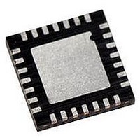
PIC16LF723A-I/ML Microchip Technology, PIC16LF723A-I/ML Datasheet - Page 68

PIC16LF723A-I/ML
Manufacturer Part Number
PIC16LF723A-I/ML
Description
MCU PIC 3.5K FLASH XLP 28-QFN
Manufacturer
Microchip Technology
Series
PIC® XLP™ 16Fr
Specifications of PIC16LF723A-I/ML
Core Size
8-Bit
Program Memory Size
7KB (4K x 14)
Peripherals
Brown-out Detect/Reset, POR, PWM, WDT
Core Processor
PIC
Speed
20MHz
Connectivity
I²C, SPI, UART/USART
Number Of I /o
25
Program Memory Type
FLASH
Ram Size
192 x 8
Voltage - Supply (vcc/vdd)
1.8 V ~ 3.6 V
Data Converters
A/D 11x8b
Oscillator Type
Internal
Operating Temperature
-40°C ~ 85°C
Package / Case
28-VQFN Exposed Pad, 28-HVQFN, 28-SQFN, 28-DHVQFN
Controller Family/series
PIC16LF
No. Of I/o's
25
Ram Memory Size
192Byte
Cpu Speed
20MHz
No. Of Timers
3
Lead Free Status / RoHS Status
Lead free / RoHS Compliant
Eeprom Size
-
Lead Free Status / RoHS Status
Lead free / RoHS Compliant, Lead free / RoHS Compliant
- Current page: 68 of 284
- Download datasheet (3Mb)
PIC16F/LF722A/723A
6.4.1
Figure 6-13 shows the diagram for this pin. This pin is
configurable to function as one of the following:
• General purpose I/O
• Timer1 oscillator output
• Timer1 clock input
6.4.2
Figure 6-14 shows the diagram for this pin. This pin is
configurable to function as one of the following:
• General purpose I/O
• Timer1 oscillator input
• Capture 2 input, Compare 2 output, and PWM2
6.4.3
Figure 6-15 shows the diagram for this pin. This pin is
configurable to function as one of the following:
• General purpose I/O
• Capture 1 input, Compare 1 output, and PWM1
6.4.4
Figure 6-16 shows the diagram for this pin. This pin is
configurable to function as one of the following:
• General purpose I/O
• SPI clock
• I
6.4.5
Figure 6-17 shows the diagram for this pin. This pin is
configurable to function as one of the following:
• General purpose I/O
• SPI data input
• I
6.4.6
Figure 6-18 shows the diagram for this pin. This pin is
configurable to function as one of the following:
• General purpose I/O
• SPI data output
6.4.7
Figure 6-19 shows the diagram for this pin. This pin is
configurable to function as one of the following:
• General purpose I/O
• Asynchronous serial output
• Synchronous clock I/O
DS41417A-page 68
output
Note:
output
2
2
C™ clock
C data I/O
RC0/T1OSO/T1CKI
RC1/T1OSI/CCP2
CCP2 pin location may be selected as
RB3 or RC1.
RC2/CCP1
RC3/SCK/SCL
RC4/SDI/SDA
RC5/SDO
RC6/TX/CK
6.4.8
Figure 6-20 shows the diagram for this pin. This pin is
configurable to function as one of the following:
• General purpose I/O
• Asynchronous serial input
• Synchronous serial data I/O
RC7/RX/DT
2010 Microchip Technology Inc.
Related parts for PIC16LF723A-I/ML
Image
Part Number
Description
Manufacturer
Datasheet
Request
R

Part Number:
Description:
IC PIC MCU FLASH 8KX14 28-SPDIP
Manufacturer:
Microchip Technology
Datasheet:

Part Number:
Description:
IC PIC MCU FLASH 8KX14 28-QFN
Manufacturer:
Microchip Technology
Datasheet:

Part Number:
Description:
IC PIC MCU FLASH 8KX14 28-SPDIP
Manufacturer:
Microchip Technology
Datasheet:

Part Number:
Description:
IC PIC MCU FLASH 8KX14 28-QFN
Manufacturer:
Microchip Technology
Datasheet:

Part Number:
Description:
IC PIC MCU FLASH 8KX14 28-SOIC
Manufacturer:
Microchip Technology
Datasheet:

Part Number:
Description:
IC PIC MCU FLASH 8KX14 28-SSOP
Manufacturer:
Microchip Technology
Datasheet:

Part Number:
Description:
IC PIC MCU FLASH 8KX14 28-SSOP
Manufacturer:
Microchip Technology
Datasheet:

Part Number:
Description:
7 KB Flash, 16 MHz Int. Osc, NanoWatt XLP 28 SOIC .300in TUBE
Manufacturer:
Microchip Technology
Datasheet:

Part Number:
Description:
IC PIC MCU FLASH 2KX14 28SOIC
Manufacturer:
Microchip Technology
Datasheet:

Part Number:
Description:
IC PIC MCU FLASH 2KX14 28QFN
Manufacturer:
Microchip Technology
Datasheet:

Part Number:
Description:
IC PIC MCU FLASH 2KX14 28DIP
Manufacturer:
Microchip Technology
Datasheet:

Part Number:
Description:
IC MCU FLASH 2KX14 28SOIC
Manufacturer:
Microchip Technology

Part Number:
Description:
IC PIC MCU FLASH 2KX14 28QFN
Manufacturer:
Microchip Technology

Part Number:
Description:
IC PIC MCU FLASH 2KX14 28SSOP
Manufacturer:
Microchip Technology
Datasheet:

Part Number:
Description:
IC, 8BIT MCU, PIC16LF, 32MHZ, QFN-28
Manufacturer:
Microchip Technology
Datasheet:


