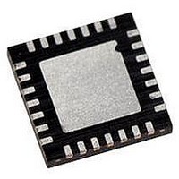
PIC16LF723A-I/ML Microchip Technology, PIC16LF723A-I/ML Datasheet - Page 91

PIC16LF723A-I/ML
Manufacturer Part Number
PIC16LF723A-I/ML
Description
MCU PIC 3.5K FLASH XLP 28-QFN
Manufacturer
Microchip Technology
Series
PIC® XLP™ 16Fr
Specifications of PIC16LF723A-I/ML
Core Size
8-Bit
Program Memory Size
7KB (4K x 14)
Peripherals
Brown-out Detect/Reset, POR, PWM, WDT
Core Processor
PIC
Speed
20MHz
Connectivity
I²C, SPI, UART/USART
Number Of I /o
25
Program Memory Type
FLASH
Ram Size
192 x 8
Voltage - Supply (vcc/vdd)
1.8 V ~ 3.6 V
Data Converters
A/D 11x8b
Oscillator Type
Internal
Operating Temperature
-40°C ~ 85°C
Package / Case
28-VQFN Exposed Pad, 28-HVQFN, 28-SQFN, 28-DHVQFN
Controller Family/series
PIC16LF
No. Of I/o's
25
Ram Memory Size
192Byte
Cpu Speed
20MHz
No. Of Timers
3
Lead Free Status / RoHS Status
Lead free / RoHS Compliant
Eeprom Size
-
Lead Free Status / RoHS Status
Lead free / RoHS Compliant, Lead free / RoHS Compliant
- Current page: 91 of 284
- Download datasheet (3Mb)
9.2.6
This is an example procedure for using the ADC to
perform an Analog-to-Digital conversion:
1.
2.
3.
4.
5.
6.
7.
8.
2010 Microchip Technology Inc.
Note 1: The global interrupt can be disabled if the
Configure Port:
• Disable pin output driver (Refer to the TRIS
• Configure pin as analog (Refer to the ANSEL
Configure the ADC module:
• Select ADC conversion clock
• Configure voltage reference
• Select ADC input channel
• Turn on ADC module
Configure ADC interrupt (optional):
• Clear ADC interrupt flag
• Enable ADC interrupt
• Enable peripheral interrupt
• Enable global interrupt
Wait the required acquisition time
Start conversion by setting the GO/DONE bit.
Wait for ADC conversion to complete by one of
the following:
• Polling the GO/DONE bit
• Waiting for the ADC interrupt (interrupts
Read ADC Result.
Clear the ADC interrupt flag (required if interrupt
is enabled).
register)
register)
enabled)
2: Refer to Section 9.3 “A/D Acquisition
A/D CONVERSION PROCEDURE
user is attempting to wake-up from Sleep
and resume in-line code execution.
Requirements”.
(1)
(2)
.
PIC16F/LF722A/723A
EXAMPLE 9-1:
;This code block configures the ADC
;for polling, Vdd reference, Frc clock
;and AN0 input.
;
;Conversion start & polling for completion
; are included.
;
BANKSEL
MOVLW
MOVWF
BANKSEL
BSF
BANKSEL
BSF
BANKSEL
MOVLW
MOVWF
CALL
BSF
BTFSC
GOTO
BANKSEL
MOVF
MOVWF
ADCON1
B’01110000’ ;ADC Frc clock,
ADCON1
TRISA
TRISA,0
ANSELA
ANSELA,0
ADCON0
B’00000001’;AN0, On
ADCON0
SampleTime ;Acquisiton delay
ADCON0,GO
ADCON0,GO
$-1
ADRES
ADRES,W
RESULT
A/D CONVERSION
;
;V
;
;
;Set RA0 to input
;
;Set RA0 to analog
;
;
;Start conversion
;Is conversion done?
;No, test again
;
;Read result
;store in GPR space
DD
reference
DS41417A-page 91
Related parts for PIC16LF723A-I/ML
Image
Part Number
Description
Manufacturer
Datasheet
Request
R

Part Number:
Description:
IC PIC MCU FLASH 8KX14 28-SPDIP
Manufacturer:
Microchip Technology
Datasheet:

Part Number:
Description:
IC PIC MCU FLASH 8KX14 28-QFN
Manufacturer:
Microchip Technology
Datasheet:

Part Number:
Description:
IC PIC MCU FLASH 8KX14 28-SPDIP
Manufacturer:
Microchip Technology
Datasheet:

Part Number:
Description:
IC PIC MCU FLASH 8KX14 28-QFN
Manufacturer:
Microchip Technology
Datasheet:

Part Number:
Description:
IC PIC MCU FLASH 8KX14 28-SOIC
Manufacturer:
Microchip Technology
Datasheet:

Part Number:
Description:
IC PIC MCU FLASH 8KX14 28-SSOP
Manufacturer:
Microchip Technology
Datasheet:

Part Number:
Description:
IC PIC MCU FLASH 8KX14 28-SSOP
Manufacturer:
Microchip Technology
Datasheet:

Part Number:
Description:
7 KB Flash, 16 MHz Int. Osc, NanoWatt XLP 28 SOIC .300in TUBE
Manufacturer:
Microchip Technology
Datasheet:

Part Number:
Description:
IC PIC MCU FLASH 2KX14 28SOIC
Manufacturer:
Microchip Technology
Datasheet:

Part Number:
Description:
IC PIC MCU FLASH 2KX14 28QFN
Manufacturer:
Microchip Technology
Datasheet:

Part Number:
Description:
IC PIC MCU FLASH 2KX14 28DIP
Manufacturer:
Microchip Technology
Datasheet:

Part Number:
Description:
IC MCU FLASH 2KX14 28SOIC
Manufacturer:
Microchip Technology

Part Number:
Description:
IC PIC MCU FLASH 2KX14 28QFN
Manufacturer:
Microchip Technology

Part Number:
Description:
IC PIC MCU FLASH 2KX14 28SSOP
Manufacturer:
Microchip Technology
Datasheet:

Part Number:
Description:
IC, 8BIT MCU, PIC16LF, 32MHZ, QFN-28
Manufacturer:
Microchip Technology
Datasheet:


