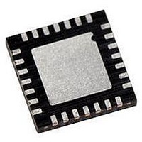
PIC16LF723A-I/ML Microchip Technology, PIC16LF723A-I/ML Datasheet - Page 130

PIC16LF723A-I/ML
Manufacturer Part Number
PIC16LF723A-I/ML
Description
MCU PIC 3.5K FLASH XLP 28-QFN
Manufacturer
Microchip Technology
Series
PIC® XLP™ 16Fr
Specifications of PIC16LF723A-I/ML
Core Size
8-Bit
Program Memory Size
7KB (4K x 14)
Peripherals
Brown-out Detect/Reset, POR, PWM, WDT
Core Processor
PIC
Speed
20MHz
Connectivity
I²C, SPI, UART/USART
Number Of I /o
25
Program Memory Type
FLASH
Ram Size
192 x 8
Voltage - Supply (vcc/vdd)
1.8 V ~ 3.6 V
Data Converters
A/D 11x8b
Oscillator Type
Internal
Operating Temperature
-40°C ~ 85°C
Package / Case
28-VQFN Exposed Pad, 28-HVQFN, 28-SQFN, 28-DHVQFN
Controller Family/series
PIC16LF
No. Of I/o's
25
Ram Memory Size
192Byte
Cpu Speed
20MHz
No. Of Timers
3
Lead Free Status / RoHS Status
Lead free / RoHS Compliant
Eeprom Size
-
Lead Free Status / RoHS Status
Lead free / RoHS Compliant, Lead free / RoHS Compliant
- Current page: 130 of 284
- Download datasheet (3Mb)
PIC16F/LF722A/723A
15.3.2
The PWM period is specified by the PR2 register of
Timer2. The PWM period can be calculated using the
formula of Equation 15-1.
EQUATION 15-1:
When TMR2 is equal to PR2, the following three events
occur on the next increment cycle:
• TMR2 is cleared
• The CCPx pin is set. (Exception: If the PWM duty
• The PWM duty cycle is latched from CCPRxL into
15.3.3
The PWM duty cycle is specified by writing a 10-bit value
to multiple registers: CCPRxL register and DCxB<1:0>
bits of the CCPxCON register. The CCPRxL contains
the eight MSbs and the DCxB<1:0> bits of the
CCPxCON register contain the two LSbs. CCPRxL and
DCxB<1:0> bits of the CCPxCON register can be written
to at any time. The duty cycle value is not latched into
CCPRxH until after the period completes (i.e., a match
between PR2 and TMR2 registers occurs). While using
the PWM, the CCPRxH register is read-only.
Equation 15-2 is used to calculate the PWM pulse
width.
Equation 15-3 is used to calculate the PWM duty cycle
ratio.
DS41417A-page 130
cycle = 0%, the pin will not be set.)
CCPRxH.
Note:
Note:
PWM Period
PWM PERIOD
The
Section 13.1 “Timer2 Operation”) is not
used in the determination of the PWM
frequency.
PWM DUTY CYCLE
T
OSC
Timer2
=
= 1/F
(TMR2 Prescale Value)
PWM PERIOD
PR2
OSC
+
postscaler
1
4 T
OSC
(refer
to
EQUATION 15-2:
EQUATION 15-3:
The CCPRxH register and a 2-bit internal latch are
used to double buffer the PWM duty cycle. This double
buffering is essential for glitchless PWM operation.
The 8-bit timer TMR2 register is concatenated with
either the 2-bit internal system clock (F
the prescaler, to create the 10-bit time base. The system
clock is used if the Timer2 prescaler is set to 1:1.
When the 10-bit time base matches the CCPRxH and
2-bit latch, then the CCPx pin is cleared (refer to
Figure 15-3).
Duty Cycle Ratio
Pulse Width
Note: T
OSC
=
= 1/F
T
=
CCPRxL:CCPxCON<5:4>
OSC
OSC
PULSE WIDTH
DUTY CYCLE RATIO
---------------------------------------------------------------------- -
CCPRxL:CCPxCON<5:4>
2010 Microchip Technology Inc.
(TMR2 Prescale Value)
4 PR2
+
OSC
1
), or 2 bits of
Related parts for PIC16LF723A-I/ML
Image
Part Number
Description
Manufacturer
Datasheet
Request
R

Part Number:
Description:
IC PIC MCU FLASH 8KX14 28-SPDIP
Manufacturer:
Microchip Technology
Datasheet:

Part Number:
Description:
IC PIC MCU FLASH 8KX14 28-QFN
Manufacturer:
Microchip Technology
Datasheet:

Part Number:
Description:
IC PIC MCU FLASH 8KX14 28-SPDIP
Manufacturer:
Microchip Technology
Datasheet:

Part Number:
Description:
IC PIC MCU FLASH 8KX14 28-QFN
Manufacturer:
Microchip Technology
Datasheet:

Part Number:
Description:
IC PIC MCU FLASH 8KX14 28-SOIC
Manufacturer:
Microchip Technology
Datasheet:

Part Number:
Description:
IC PIC MCU FLASH 8KX14 28-SSOP
Manufacturer:
Microchip Technology
Datasheet:

Part Number:
Description:
IC PIC MCU FLASH 8KX14 28-SSOP
Manufacturer:
Microchip Technology
Datasheet:

Part Number:
Description:
7 KB Flash, 16 MHz Int. Osc, NanoWatt XLP 28 SOIC .300in TUBE
Manufacturer:
Microchip Technology
Datasheet:

Part Number:
Description:
IC PIC MCU FLASH 2KX14 28SOIC
Manufacturer:
Microchip Technology
Datasheet:

Part Number:
Description:
IC PIC MCU FLASH 2KX14 28QFN
Manufacturer:
Microchip Technology
Datasheet:

Part Number:
Description:
IC PIC MCU FLASH 2KX14 28DIP
Manufacturer:
Microchip Technology
Datasheet:

Part Number:
Description:
IC MCU FLASH 2KX14 28SOIC
Manufacturer:
Microchip Technology

Part Number:
Description:
IC PIC MCU FLASH 2KX14 28QFN
Manufacturer:
Microchip Technology

Part Number:
Description:
IC PIC MCU FLASH 2KX14 28SSOP
Manufacturer:
Microchip Technology
Datasheet:

Part Number:
Description:
IC, 8BIT MCU, PIC16LF, 32MHZ, QFN-28
Manufacturer:
Microchip Technology
Datasheet:


