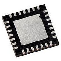
PIC16LF723A-I/ML Microchip Technology, PIC16LF723A-I/ML Datasheet - Page 167

PIC16LF723A-I/ML
Manufacturer Part Number
PIC16LF723A-I/ML
Description
MCU PIC 3.5K FLASH XLP 28-QFN
Manufacturer
Microchip Technology
Series
PIC® XLP™ 16Fr
Specifications of PIC16LF723A-I/ML
Core Size
8-Bit
Program Memory Size
7KB (4K x 14)
Peripherals
Brown-out Detect/Reset, POR, PWM, WDT
Core Processor
PIC
Speed
20MHz
Connectivity
I²C, SPI, UART/USART
Number Of I /o
25
Program Memory Type
FLASH
Ram Size
192 x 8
Voltage - Supply (vcc/vdd)
1.8 V ~ 3.6 V
Data Converters
A/D 11x8b
Oscillator Type
Internal
Operating Temperature
-40°C ~ 85°C
Package / Case
28-VQFN Exposed Pad, 28-HVQFN, 28-SQFN, 28-DHVQFN
Controller Family/series
PIC16LF
No. Of I/o's
25
Ram Memory Size
192Byte
Cpu Speed
20MHz
No. Of Timers
3
Lead Free Status / RoHS Status
Lead free / RoHS Compliant
Eeprom Size
-
Lead Free Status / RoHS Status
Lead free / RoHS Compliant, Lead free / RoHS Compliant
- Current page: 167 of 284
- Download datasheet (3Mb)
17.2.4
Once the SSP module has been enabled, it waits for a
Start condition to occur. Following the Start condition,
the 8 bits are shifted into the SSPSR register. All
incoming bits are sampled with the rising edge of the
clock line (SCL).
17.2.4.1
In 7-bit Addressing mode (Figure 17-10), the value of
register SSPSR<7:1> is compared to the value of reg-
ister SSPADD<7:1>. The address is compared on the
falling edge of the eighth clock (SCL) pulse. If the
addresses match, and the BF and SSPOV bits are
clear, the following events occur:
• The SSPSR register value is loaded into the
• The BF bit is set.
• An ACK pulse is generated.
• SSP interrupt flag bit, SSPIF of the PIR1 register,
2010 Microchip Technology Inc.
SSPBUF register.
is set (interrupt is generated if enabled) on the
falling edge of the ninth SCL pulse.
ADDRESSING
7-bit Addressing
PIC16F/LF722A/723A
17.2.4.2
In 10-bit Address mode, two address bytes need to be
received by the slave (Figure 17-11). The five Most
Significant bits (MSbs) of the first address byte specify
if it is a 10-bit address. The R/W bit of the SSPSTAT
register must specify a write so the slave device will
receive the second address byte. For a 10-bit address,
the first byte would equal ‘1111 0 A9 A8 0’, where
A9 and A8 are the two MSbs of the address.
The sequence of events for 10-bit address is as follows
for reception:
1.
2.
3.
4.
5.
6.
7.
8.
9.
If data is requested by the master, once the slave has
been addressed:
1.
2.
3.
4.
5.
17.2.4.3
The Address Masking register (SSPMSK) is only
accessible while the SSPM bits of the SSPCON
register are set to ‘1001’. In this register, the user can
select which bits of a received address the hardware
will compare when determining an address match. Any
bit that is set to a zero in the SSPMSK register, the
corresponding bit in the received address byte and
SSPADD register are ignored when determining an
address match. By default, the register is set to all
ones, requiring a complete match of a 7-bit address or
the lower eight bits of a 10-bit address.
Load SSPADD register with high byte of address.
Receive first (high) byte of address (bits SSPIF,
BF and UA of the SSPSTAT register are set).
Read the SSPBUF register (clears bit BF).
Clear the SSPIF flag bit.
Update the SSPADD register with second (low)
byte of address (clears UA bit and releases the
SCL line).
Receive low byte of address (bits SSPIF, BF and
UA are set).
Update the SSPADD register with the high byte
of address. If match releases SCL line, this will
clear bit UA.
Read the SSPBUF register (clears bit BF).
Clear flag bit SSPIF.
Receive repeated Start condition.
Receive repeat of high byte address with R/W = 1,
indicating a read.
BF bit is set and the CKP bit is cleared, stopping
SCL and indicating a read request.
SSPBUF is written, setting BF, with the data to
send to the master device.
CKP is set in software, releasing the SCL line.
10-bit Addressing
Address Masking
DS41417A-page 167
Related parts for PIC16LF723A-I/ML
Image
Part Number
Description
Manufacturer
Datasheet
Request
R

Part Number:
Description:
IC PIC MCU FLASH 8KX14 28-SPDIP
Manufacturer:
Microchip Technology
Datasheet:

Part Number:
Description:
IC PIC MCU FLASH 8KX14 28-QFN
Manufacturer:
Microchip Technology
Datasheet:

Part Number:
Description:
IC PIC MCU FLASH 8KX14 28-SPDIP
Manufacturer:
Microchip Technology
Datasheet:

Part Number:
Description:
IC PIC MCU FLASH 8KX14 28-QFN
Manufacturer:
Microchip Technology
Datasheet:

Part Number:
Description:
IC PIC MCU FLASH 8KX14 28-SOIC
Manufacturer:
Microchip Technology
Datasheet:

Part Number:
Description:
IC PIC MCU FLASH 8KX14 28-SSOP
Manufacturer:
Microchip Technology
Datasheet:

Part Number:
Description:
IC PIC MCU FLASH 8KX14 28-SSOP
Manufacturer:
Microchip Technology
Datasheet:

Part Number:
Description:
7 KB Flash, 16 MHz Int. Osc, NanoWatt XLP 28 SOIC .300in TUBE
Manufacturer:
Microchip Technology
Datasheet:

Part Number:
Description:
IC PIC MCU FLASH 2KX14 28SOIC
Manufacturer:
Microchip Technology
Datasheet:

Part Number:
Description:
IC PIC MCU FLASH 2KX14 28QFN
Manufacturer:
Microchip Technology
Datasheet:

Part Number:
Description:
IC PIC MCU FLASH 2KX14 28DIP
Manufacturer:
Microchip Technology
Datasheet:

Part Number:
Description:
IC MCU FLASH 2KX14 28SOIC
Manufacturer:
Microchip Technology

Part Number:
Description:
IC PIC MCU FLASH 2KX14 28QFN
Manufacturer:
Microchip Technology

Part Number:
Description:
IC PIC MCU FLASH 2KX14 28SSOP
Manufacturer:
Microchip Technology
Datasheet:

Part Number:
Description:
IC, 8BIT MCU, PIC16LF, 32MHZ, QFN-28
Manufacturer:
Microchip Technology
Datasheet:


