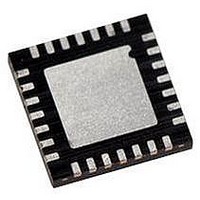
PIC16LF723A-I/ML Microchip Technology, PIC16LF723A-I/ML Datasheet - Page 23

PIC16LF723A-I/ML
Manufacturer Part Number
PIC16LF723A-I/ML
Description
MCU PIC 3.5K FLASH XLP 28-QFN
Manufacturer
Microchip Technology
Series
PIC® XLP™ 16Fr
Specifications of PIC16LF723A-I/ML
Core Size
8-Bit
Program Memory Size
7KB (4K x 14)
Peripherals
Brown-out Detect/Reset, POR, PWM, WDT
Core Processor
PIC
Speed
20MHz
Connectivity
I²C, SPI, UART/USART
Number Of I /o
25
Program Memory Type
FLASH
Ram Size
192 x 8
Voltage - Supply (vcc/vdd)
1.8 V ~ 3.6 V
Data Converters
A/D 11x8b
Oscillator Type
Internal
Operating Temperature
-40°C ~ 85°C
Package / Case
28-VQFN Exposed Pad, 28-HVQFN, 28-SQFN, 28-DHVQFN
Controller Family/series
PIC16LF
No. Of I/o's
25
Ram Memory Size
192Byte
Cpu Speed
20MHz
No. Of Timers
3
Lead Free Status / RoHS Status
Lead free / RoHS Compliant
Eeprom Size
-
Lead Free Status / RoHS Status
Lead free / RoHS Compliant, Lead free / RoHS Compliant
- Current page: 23 of 284
- Download datasheet (3Mb)
2.2.2.2
The OPTION register, shown in Register 2-2, is a
readable and writable register, which contains various
control bits to configure:
• Timer0/WDT prescaler
• External RB0/INT interrupt
• Timer0
• Weak pull-ups on PORTB
REGISTER 2-2:
2010 Microchip Technology Inc.
bit 7
Legend:
R = Readable bit
-n = Value at POR
bit 7
bit 6
bit 5
bit 4
bit 3
bit 2-0
R/W-1
RBPU
OPTION register
RBPU: PORTB Pull-up Enable bit
1 = PORTB pull-ups are disabled
0 = PORTB pull-ups are enabled by individual bits in the WPUB register
INTEDG: Interrupt Edge Select bit
1 = Interrupt on rising edge of RB0/INT pin
0 = Interrupt on falling edge of RB0/INT pin
T0CS: Timer0 Clock Source Select bit
1 = Transition on RA4/T0CKI pin
0 = Internal instruction cycle clock (F
T0SE: Timer0 Source Edge Select bit
1 = Increment on high-to-low transition on RA4/T0CKI pin
0 = Increment on low-to-high transition on RA4/T0CKI pin
PSA: Prescaler Assignment bit
1 = Prescaler is assigned to the WDT
0 = Prescaler is assigned to the Timer0 module
PS<2:0>: Prescaler Rate Select bits
INTEDG
R/W-1
OPTION_REG: OPTION REGISTER
Bit Value
000
001
010
011
100
101
110
111
W = Writable bit
‘1’ = Bit is set
R/W-1
T0CS
Timer0 Rate
1 : 2
1 : 4
1 : 8
1 : 16
1 : 32
1 : 64
1 : 128
1 : 256
R/W-1
T0SE
WDT Rate
1 : 1
1 : 2
1 : 4
1 : 8
1 : 16
1 : 32
1 : 64
1 : 128
OSC
/4)
U = Unimplemented bit, read as ‘0’
‘0’ = Bit is cleared
PIC16F/LF722A/723A
R/W-1
PSA
Note:
To achieve a 1:1 prescaler assignment for
Timer0, assign the prescaler to the WDT
by setting PSA bit of the OPTION register
to ‘1’. Refer to Section 12.3 “Timer1
Prescaler”.
R/W-1
PS2
x = Bit is unknown
R/W-1
PS1
DS41417A-page 23
R/W-1
PS0
bit 0
Related parts for PIC16LF723A-I/ML
Image
Part Number
Description
Manufacturer
Datasheet
Request
R

Part Number:
Description:
IC PIC MCU FLASH 8KX14 28-SPDIP
Manufacturer:
Microchip Technology
Datasheet:

Part Number:
Description:
IC PIC MCU FLASH 8KX14 28-QFN
Manufacturer:
Microchip Technology
Datasheet:

Part Number:
Description:
IC PIC MCU FLASH 8KX14 28-SPDIP
Manufacturer:
Microchip Technology
Datasheet:

Part Number:
Description:
IC PIC MCU FLASH 8KX14 28-QFN
Manufacturer:
Microchip Technology
Datasheet:

Part Number:
Description:
IC PIC MCU FLASH 8KX14 28-SOIC
Manufacturer:
Microchip Technology
Datasheet:

Part Number:
Description:
IC PIC MCU FLASH 8KX14 28-SSOP
Manufacturer:
Microchip Technology
Datasheet:

Part Number:
Description:
IC PIC MCU FLASH 8KX14 28-SSOP
Manufacturer:
Microchip Technology
Datasheet:

Part Number:
Description:
7 KB Flash, 16 MHz Int. Osc, NanoWatt XLP 28 SOIC .300in TUBE
Manufacturer:
Microchip Technology
Datasheet:

Part Number:
Description:
IC PIC MCU FLASH 2KX14 28SOIC
Manufacturer:
Microchip Technology
Datasheet:

Part Number:
Description:
IC PIC MCU FLASH 2KX14 28QFN
Manufacturer:
Microchip Technology
Datasheet:

Part Number:
Description:
IC PIC MCU FLASH 2KX14 28DIP
Manufacturer:
Microchip Technology
Datasheet:

Part Number:
Description:
IC MCU FLASH 2KX14 28SOIC
Manufacturer:
Microchip Technology

Part Number:
Description:
IC PIC MCU FLASH 2KX14 28QFN
Manufacturer:
Microchip Technology

Part Number:
Description:
IC PIC MCU FLASH 2KX14 28SSOP
Manufacturer:
Microchip Technology
Datasheet:

Part Number:
Description:
IC, 8BIT MCU, PIC16LF, 32MHZ, QFN-28
Manufacturer:
Microchip Technology
Datasheet:


