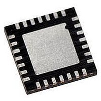
PIC16LF723A-I/ML Microchip Technology, PIC16LF723A-I/ML Datasheet - Page 170

PIC16LF723A-I/ML
Manufacturer Part Number
PIC16LF723A-I/ML
Description
MCU PIC 3.5K FLASH XLP 28-QFN
Manufacturer
Microchip Technology
Series
PIC® XLP™ 16Fr
Specifications of PIC16LF723A-I/ML
Core Size
8-Bit
Program Memory Size
7KB (4K x 14)
Peripherals
Brown-out Detect/Reset, POR, PWM, WDT
Core Processor
PIC
Speed
20MHz
Connectivity
I²C, SPI, UART/USART
Number Of I /o
25
Program Memory Type
FLASH
Ram Size
192 x 8
Voltage - Supply (vcc/vdd)
1.8 V ~ 3.6 V
Data Converters
A/D 11x8b
Oscillator Type
Internal
Operating Temperature
-40°C ~ 85°C
Package / Case
28-VQFN Exposed Pad, 28-HVQFN, 28-SQFN, 28-DHVQFN
Controller Family/series
PIC16LF
No. Of I/o's
25
Ram Memory Size
192Byte
Cpu Speed
20MHz
No. Of Timers
3
Lead Free Status / RoHS Status
Lead free / RoHS Compliant
Eeprom Size
-
Lead Free Status / RoHS Status
Lead free / RoHS Compliant, Lead free / RoHS Compliant
- Current page: 170 of 284
- Download datasheet (3Mb)
PIC16F/LF722A/723A
17.2.6
When the R/W bit of the received address byte is set
and an address match occurs, the R/W bit of the
SSPSTAT register is set and the slave will respond to
the master by reading out data. After the address match,
an ACK pulse is generated by the slave hardware and
the SCL pin is held low (clock is automatically stretched)
until the slave is ready to respond. See Section 17.2.7
“Clock Stretching”. The data the slave will transmit
must be loaded into the SSPBUF register, which sets
the BF bit. The SCL line is released by setting the CKP
bit of the SSPCON register.
An SSP interrupt is generated for each transferred data
byte. The SSPIF flag bit of the PIR1 register initiates an
SSP interrupt, and must be cleared by software before
the next byte is transmitted. The BF bit of the SSPSTAT
register is cleared on the falling edge of the 8th
received clock pulse. The SSPIF flag bit is set on the
falling edge of the ninth clock pulse.
FIGURE 17-12:
DS41417A-page 170
SDA
SCL
SSPIF
BF
CKP
S
TRANSMISSION
A7
1
Data in
sampled
A6
2
I
2
C WAVEFORMS FOR TRANSMISSION (7-BIT ADDRESS)
A5
Receiving Address
3
A4
4
Dummy read of SSPBUF
A3
5
A2
6
to clear BF flag
A1
7
R/W
8
9
ACK
responds to SSPIF
SCL held low
while CPU
Following the 8th falling clock edge, control of the SDA
line is released back to the master so that the master
can acknowledge or not acknowledge the response. If
the master sends a not acknowledge, the slave’s
transmission is complete and the slave must monitor for
the next Start condition. If the master acknowledges,
control of the bus is returned to the slave to transmit
another byte of data. Just as with the previous byte, the
clock is stretched by the slave, data must be loaded into
the SSPBUF and CKP must be set to release the clock
line (SCL).
SSPBUF is written in software From SSP Interrupt
D7
1
D6
2
Cleared in software
Set bit after writing to SSPBUF
(the SSPBUF must be written to
before the CKP bit can be set)
D5
3
D4
4
Transmitting Data
D3
5
2010 Microchip Technology Inc.
D2
6
Service Routine
D1
7
D0
8
ACK
9
P
Related parts for PIC16LF723A-I/ML
Image
Part Number
Description
Manufacturer
Datasheet
Request
R

Part Number:
Description:
IC PIC MCU FLASH 8KX14 28-SPDIP
Manufacturer:
Microchip Technology
Datasheet:

Part Number:
Description:
IC PIC MCU FLASH 8KX14 28-QFN
Manufacturer:
Microchip Technology
Datasheet:

Part Number:
Description:
IC PIC MCU FLASH 8KX14 28-SPDIP
Manufacturer:
Microchip Technology
Datasheet:

Part Number:
Description:
IC PIC MCU FLASH 8KX14 28-QFN
Manufacturer:
Microchip Technology
Datasheet:

Part Number:
Description:
IC PIC MCU FLASH 8KX14 28-SOIC
Manufacturer:
Microchip Technology
Datasheet:

Part Number:
Description:
IC PIC MCU FLASH 8KX14 28-SSOP
Manufacturer:
Microchip Technology
Datasheet:

Part Number:
Description:
IC PIC MCU FLASH 8KX14 28-SSOP
Manufacturer:
Microchip Technology
Datasheet:

Part Number:
Description:
7 KB Flash, 16 MHz Int. Osc, NanoWatt XLP 28 SOIC .300in TUBE
Manufacturer:
Microchip Technology
Datasheet:

Part Number:
Description:
IC PIC MCU FLASH 2KX14 28SOIC
Manufacturer:
Microchip Technology
Datasheet:

Part Number:
Description:
IC PIC MCU FLASH 2KX14 28QFN
Manufacturer:
Microchip Technology
Datasheet:

Part Number:
Description:
IC PIC MCU FLASH 2KX14 28DIP
Manufacturer:
Microchip Technology
Datasheet:

Part Number:
Description:
IC MCU FLASH 2KX14 28SOIC
Manufacturer:
Microchip Technology

Part Number:
Description:
IC PIC MCU FLASH 2KX14 28QFN
Manufacturer:
Microchip Technology

Part Number:
Description:
IC PIC MCU FLASH 2KX14 28SSOP
Manufacturer:
Microchip Technology
Datasheet:

Part Number:
Description:
IC, 8BIT MCU, PIC16LF, 32MHZ, QFN-28
Manufacturer:
Microchip Technology
Datasheet:


