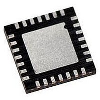
PIC16LF723A-I/ML Microchip Technology, PIC16LF723A-I/ML Datasheet - Page 59

PIC16LF723A-I/ML
Manufacturer Part Number
PIC16LF723A-I/ML
Description
MCU PIC 3.5K FLASH XLP 28-QFN
Manufacturer
Microchip Technology
Series
PIC® XLP™ 16Fr
Specifications of PIC16LF723A-I/ML
Core Size
8-Bit
Program Memory Size
7KB (4K x 14)
Peripherals
Brown-out Detect/Reset, POR, PWM, WDT
Core Processor
PIC
Speed
20MHz
Connectivity
I²C, SPI, UART/USART
Number Of I /o
25
Program Memory Type
FLASH
Ram Size
192 x 8
Voltage - Supply (vcc/vdd)
1.8 V ~ 3.6 V
Data Converters
A/D 11x8b
Oscillator Type
Internal
Operating Temperature
-40°C ~ 85°C
Package / Case
28-VQFN Exposed Pad, 28-HVQFN, 28-SQFN, 28-DHVQFN
Controller Family/series
PIC16LF
No. Of I/o's
25
Ram Memory Size
192Byte
Cpu Speed
20MHz
No. Of Timers
3
Lead Free Status / RoHS Status
Lead free / RoHS Compliant
Eeprom Size
-
Lead Free Status / RoHS Status
Lead free / RoHS Compliant, Lead free / RoHS Compliant
- Current page: 59 of 284
- Download datasheet (3Mb)
6.3.4
Each PORTB pin is multiplexed with other functions. The
pins and their combined functions are briefly described
here. For specific information about individual functions
such as the SSP, I
section in this data sheet.
6.3.4.1
Figure 6-7 shows the diagram for this pin. This pin is
configurable to function as one of the following:
• General purpose I/O
• Analog input for the ADC
• Capacitive sensing input
• External edge triggered interrupt
6.3.4.2
Figure 6-8 shows the diagram for this pin. This pin is
configurable to function as one of the following:
• General purpose I/O
• Analog input for the ADC
• Capacitive sensing input
6.3.4.3
Figure 6-8 shows the diagram for this pin. This pin is
configurable to function as one of the following:
• General purpose I/O
• Analog input for the ADC
• Capacitive sensing input
6.3.4.4
Figure 6-9 shows the diagram for this pin. This pin is
configurable to function as one of the following:
• General purpose I/O
• Analog input for the ADC
• Capacitive sensing input
• Capture 2 input, Compare 2 output, and PWM2
6.3.4.5
Figure 6-8 shows the diagram for this pin. This pin is
configurable to function as one of the following:
• General purpose I/O
• Analog input for the ADC
• Capacitive sensing input
2010 Microchip Technology Inc.
output
Note:
PIN DESCRIPTIONS AND
DIAGRAMS
CCP2 pin location may be selected as
RB3 or RC1.
RB0/AN12/CPS0/INT
RB1/AN10/CPS1
RB2/AN8/CPS2
RB3/AN9/CPS3/CCP2
RB4/AN11/CPS4
2
C or interrupts, refer to the appropriate
PIC16F/LF722A/723A
6.3.4.6
Figure 6-10 shows the diagram for this pin. This pin is
configurable to function as one of the following:
• General purpose I/O
• Analog input for the ADC
• Capacitive sensing input
• Timer1 gate input
6.3.4.7
Figure 6-11 shows the diagram for this pin. This pin is
configurable to function as one of the following:
• a general purpose I/O
• In-Circuit Serial Programming clock
6.3.4.8
Figure 6-12 shows the diagram for this pin. This pin is
configurable to function as one of the following:
• General purpose I/O
• In-Circuit Serial Programming data
RB5/AN13/CPS5/T1G
RB6/ICSPCLK
RB7/ICSPDAT
DS41417A-page 59
Related parts for PIC16LF723A-I/ML
Image
Part Number
Description
Manufacturer
Datasheet
Request
R

Part Number:
Description:
IC PIC MCU FLASH 8KX14 28-SPDIP
Manufacturer:
Microchip Technology
Datasheet:

Part Number:
Description:
IC PIC MCU FLASH 8KX14 28-QFN
Manufacturer:
Microchip Technology
Datasheet:

Part Number:
Description:
IC PIC MCU FLASH 8KX14 28-SPDIP
Manufacturer:
Microchip Technology
Datasheet:

Part Number:
Description:
IC PIC MCU FLASH 8KX14 28-QFN
Manufacturer:
Microchip Technology
Datasheet:

Part Number:
Description:
IC PIC MCU FLASH 8KX14 28-SOIC
Manufacturer:
Microchip Technology
Datasheet:

Part Number:
Description:
IC PIC MCU FLASH 8KX14 28-SSOP
Manufacturer:
Microchip Technology
Datasheet:

Part Number:
Description:
IC PIC MCU FLASH 8KX14 28-SSOP
Manufacturer:
Microchip Technology
Datasheet:

Part Number:
Description:
7 KB Flash, 16 MHz Int. Osc, NanoWatt XLP 28 SOIC .300in TUBE
Manufacturer:
Microchip Technology
Datasheet:

Part Number:
Description:
IC PIC MCU FLASH 2KX14 28SOIC
Manufacturer:
Microchip Technology
Datasheet:

Part Number:
Description:
IC PIC MCU FLASH 2KX14 28QFN
Manufacturer:
Microchip Technology
Datasheet:

Part Number:
Description:
IC PIC MCU FLASH 2KX14 28DIP
Manufacturer:
Microchip Technology
Datasheet:

Part Number:
Description:
IC MCU FLASH 2KX14 28SOIC
Manufacturer:
Microchip Technology

Part Number:
Description:
IC PIC MCU FLASH 2KX14 28QFN
Manufacturer:
Microchip Technology

Part Number:
Description:
IC PIC MCU FLASH 2KX14 28SSOP
Manufacturer:
Microchip Technology
Datasheet:

Part Number:
Description:
IC, 8BIT MCU, PIC16LF, 32MHZ, QFN-28
Manufacturer:
Microchip Technology
Datasheet:


