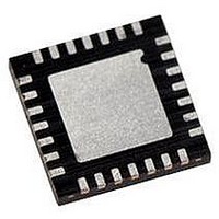
PIC16LF723A-I/ML Microchip Technology, PIC16LF723A-I/ML Datasheet - Page 159

PIC16LF723A-I/ML
Manufacturer Part Number
PIC16LF723A-I/ML
Description
MCU PIC 3.5K FLASH XLP 28-QFN
Manufacturer
Microchip Technology
Series
PIC® XLP™ 16Fr
Specifications of PIC16LF723A-I/ML
Core Size
8-Bit
Program Memory Size
7KB (4K x 14)
Peripherals
Brown-out Detect/Reset, POR, PWM, WDT
Core Processor
PIC
Speed
20MHz
Connectivity
I²C, SPI, UART/USART
Number Of I /o
25
Program Memory Type
FLASH
Ram Size
192 x 8
Voltage - Supply (vcc/vdd)
1.8 V ~ 3.6 V
Data Converters
A/D 11x8b
Oscillator Type
Internal
Operating Temperature
-40°C ~ 85°C
Package / Case
28-VQFN Exposed Pad, 28-HVQFN, 28-SQFN, 28-DHVQFN
Controller Family/series
PIC16LF
No. Of I/o's
25
Ram Memory Size
192Byte
Cpu Speed
20MHz
No. Of Timers
3
Lead Free Status / RoHS Status
Lead free / RoHS Compliant
Eeprom Size
-
Lead Free Status / RoHS Status
Lead free / RoHS Compliant, Lead free / RoHS Compliant
- Current page: 159 of 284
- Download datasheet (3Mb)
17.1.2
For any SPI device acting as a slave, the data is
transmitted and received as external clock pulses
appear on SCK pin. This external clock must meet the
minimum high and low times as specified in the
electrical specifications.
17.1.2.1
The SSP consists of a transmit/receive shift register
(SSPSR) and a buffer register (SSPBUF). The SSPSR
shifts the data in and out of the device, MSb first. The
SSPBUF holds the data that was written to the SSPSR
until the received data is ready.
The slave has no control as to when data will be
clocked in or out of the device. All data that is to be
transmitted, to a master or another slave, must be
loaded into the SSPBUF register before the first clock
pulse is received.
Once eight bits of data have been received:
• Received byte is moved to the SSPBUF register
• BF bit of the SSPSTAT register is set
• SSPIF bit of the PIR1 register is set
Any write to the SSPBUF register during transmission/
reception of data will be ignored and the Write Collision
Detect bit, WCOL of the SSPCON register, will be set.
User software must clear the WCOL bit so that it can be
determined if the following write(s) to the SSPBUF
register completed successfully.
The user’s firmware must read SSPBUF, clearing the
BF flag, or the SSPOV bit of the SSPCON register will
be set with the reception of the next byte and
communication will be disabled.
A SPI module transmits and receives at the same time,
occasionally causing dummy data to be transmitted/
received. It is up to the user to determine which data is
to be used and what can be discarded.
2010 Microchip Technology Inc.
SLAVE MODE
Slave Mode Operation
PIC16F/LF722A/723A
17.1.2.2
To enable the serial port, the SSPEN bit of the
SSPCON register must be set. If a Slave mode of
operation is selected in the SSPM bits of the SSPCON
register, the SDI, SDO and SCK pins will be assigned
as serial port pins.
For these pins to function as serial port pins, they must
have their corresponding data direction bits set or
cleared in the associated TRIS register as follows:
• SDI configured as input
• SDO configured as output
• SCK configured as input
Optionally, a fourth pin, Slave Select (SS) may be used
in Slave mode. Slave Select may be configured to
operate on one of the following pins via the SSSEL bit in
the APFCON register.
• RA5/AN4/SS
• RA0/AN0/SS
Upon selection of a Slave Select pin, the appropriate
bits must be set in the ANSELA and TRISA registers.
Slave Select must be set as an input by setting the
corresponding bit in TRISA, and digital I/O must be
enabled on the SS pin by clearing the corresponding bit
of the ANSELA register.
17.1.2.3
When initializing the SSP module to SPI Slave mode,
compatibility must be ensured with the master device.
This is done by programming the appropriate control
bits of the SSPCON and SSPSTAT registers. These
control bits allow the following to be specified:
• SCK as clock input
• Idle state of SCK (CKP bit)
• Data input sample phase (SMP bit)
• Output data on rising/falling edge of SCK (CKE bit)
Figure 17-4 and Figure 17-5 show example waveforms
of Slave mode operation.
Enabling Slave I/O
Slave Mode Setup
DS41417A-page 159
Related parts for PIC16LF723A-I/ML
Image
Part Number
Description
Manufacturer
Datasheet
Request
R

Part Number:
Description:
IC PIC MCU FLASH 8KX14 28-SPDIP
Manufacturer:
Microchip Technology
Datasheet:

Part Number:
Description:
IC PIC MCU FLASH 8KX14 28-QFN
Manufacturer:
Microchip Technology
Datasheet:

Part Number:
Description:
IC PIC MCU FLASH 8KX14 28-SPDIP
Manufacturer:
Microchip Technology
Datasheet:

Part Number:
Description:
IC PIC MCU FLASH 8KX14 28-QFN
Manufacturer:
Microchip Technology
Datasheet:

Part Number:
Description:
IC PIC MCU FLASH 8KX14 28-SOIC
Manufacturer:
Microchip Technology
Datasheet:

Part Number:
Description:
IC PIC MCU FLASH 8KX14 28-SSOP
Manufacturer:
Microchip Technology
Datasheet:

Part Number:
Description:
IC PIC MCU FLASH 8KX14 28-SSOP
Manufacturer:
Microchip Technology
Datasheet:

Part Number:
Description:
7 KB Flash, 16 MHz Int. Osc, NanoWatt XLP 28 SOIC .300in TUBE
Manufacturer:
Microchip Technology
Datasheet:

Part Number:
Description:
IC PIC MCU FLASH 2KX14 28SOIC
Manufacturer:
Microchip Technology
Datasheet:

Part Number:
Description:
IC PIC MCU FLASH 2KX14 28QFN
Manufacturer:
Microchip Technology
Datasheet:

Part Number:
Description:
IC PIC MCU FLASH 2KX14 28DIP
Manufacturer:
Microchip Technology
Datasheet:

Part Number:
Description:
IC MCU FLASH 2KX14 28SOIC
Manufacturer:
Microchip Technology

Part Number:
Description:
IC PIC MCU FLASH 2KX14 28QFN
Manufacturer:
Microchip Technology

Part Number:
Description:
IC PIC MCU FLASH 2KX14 28SSOP
Manufacturer:
Microchip Technology
Datasheet:

Part Number:
Description:
IC, 8BIT MCU, PIC16LF, 32MHZ, QFN-28
Manufacturer:
Microchip Technology
Datasheet:


