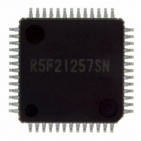
R5F21257SNFP#U0 Renesas Electronics America, R5F21257SNFP#U0 Datasheet - Page 199

R5F21257SNFP#U0
Manufacturer Part Number
R5F21257SNFP#U0
Description
IC R8C/25 MCU FLASH 52LQFP
Manufacturer
Renesas Electronics America
Series
R8C/2x/25r
Specifications of R5F21257SNFP#U0
Core Processor
R8C
Core Size
16/32-Bit
Speed
20MHz
Connectivity
I²C, LIN, SIO, SSU, UART/USART
Peripherals
POR, Voltage Detect, WDT
Number Of I /o
41
Program Memory Size
48KB (48K x 8)
Program Memory Type
FLASH
Ram Size
2.5K x 8
Voltage - Supply (vcc/vdd)
2.2 V ~ 5.5 V
Data Converters
A/D 12x10b
Oscillator Type
Internal
Operating Temperature
-20°C ~ 85°C
Package / Case
52-LQFP
For Use With
R0K521256S000BE - KIT EVAL STARTER FOR R8C/25
Lead Free Status / RoHS Status
Lead free / RoHS Compliant
Eeprom Size
-
Available stocks
Company
Part Number
Manufacturer
Quantity
Price
- Current page: 199 of 527
- Download datasheet (6Mb)
R8C/24 Group, R8C/25 Group
Rev.3.00
REJ09B0244-0300
14.3.4
In the output compare function, PWM mode, reset synchronous PWM mode, complementary PWM mode, and
PWM3 mode, the TRDIOji (i = 0 or 1, j = either A, B, C, or D) output pin can be forcibly set to a programmable
I/O port by the INT0 pin input, and pulse output can be cut off.
The pins used for output in these functions or modes can function as the output pin of timer RD when the
applicable bit in the TRDOER1 register is set to 0 (enable timer RD output). When the PTO bit in the
TRDOER2 register to 1 (INT0 of pulse output forced cutoff signal input enabled), all bits in the TRDOER1
register are set to 1 (disable timer RD output, the TRDIOji output pin is used as the programmable I/O port)
after “L” is applied to the INT0 pin. The TRDIOji output pin is set to the programmable I/O port after “L” is
applied to the INT0 pin and waiting for 1 to 2 cycles of the timer RD operation clock (refer to Table 14.11
Timer RD Operation Clocks).
Set as below when using this function:
According to the selection of the POL bit in the INT0IC register and change of the INT0 pin input, the IR bit in
the INT0IC register is set to 1 (interrupt request). Refer to 12. Interrupts for details of interrupts.
• Set the pin status (high impedance, “L” or “H” output) to pulse output forced cutoff by registers P2 and
• Set the INT0EN bit in the INTEN register to 1 (enable INT0 input) and the INT0PL bit to 0 (one edge).
• Set the PD4_5 bit in the PD4 register to 0 (input mode).
• Set the INT0 digital filter by bits INT0F1 to INT0F0 in the INTF register.
• Set the PTO bit in the TRDOER2 register to 1 (enable pulse output forced cutoff signal input INT0).
Feb 29, 2008
PD2.
Pulse Output Forced Cutoff
Page 180 of 485
14. Timers
Related parts for R5F21257SNFP#U0
Image
Part Number
Description
Manufacturer
Datasheet
Request
R

Part Number:
Description:
KIT STARTER FOR M16C/29
Manufacturer:
Renesas Electronics America
Datasheet:

Part Number:
Description:
KIT STARTER FOR R8C/2D
Manufacturer:
Renesas Electronics America
Datasheet:

Part Number:
Description:
R0K33062P STARTER KIT
Manufacturer:
Renesas Electronics America
Datasheet:

Part Number:
Description:
KIT STARTER FOR R8C/23 E8A
Manufacturer:
Renesas Electronics America
Datasheet:

Part Number:
Description:
KIT STARTER FOR R8C/25
Manufacturer:
Renesas Electronics America
Datasheet:

Part Number:
Description:
KIT STARTER H8S2456 SHARPE DSPLY
Manufacturer:
Renesas Electronics America
Datasheet:

Part Number:
Description:
KIT STARTER FOR R8C38C
Manufacturer:
Renesas Electronics America
Datasheet:

Part Number:
Description:
KIT STARTER FOR R8C35C
Manufacturer:
Renesas Electronics America
Datasheet:

Part Number:
Description:
KIT STARTER FOR R8CL3AC+LCD APPS
Manufacturer:
Renesas Electronics America
Datasheet:

Part Number:
Description:
KIT STARTER FOR RX610
Manufacturer:
Renesas Electronics America
Datasheet:

Part Number:
Description:
KIT STARTER FOR R32C/118
Manufacturer:
Renesas Electronics America
Datasheet:

Part Number:
Description:
KIT DEV RSK-R8C/26-29
Manufacturer:
Renesas Electronics America
Datasheet:

Part Number:
Description:
KIT STARTER FOR SH7124
Manufacturer:
Renesas Electronics America
Datasheet:

Part Number:
Description:
KIT STARTER FOR H8SX/1622
Manufacturer:
Renesas Electronics America
Datasheet:

Part Number:
Description:
KIT DEV FOR SH7203
Manufacturer:
Renesas Electronics America
Datasheet:


