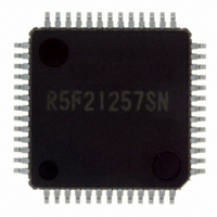
R5F21257SNFP#U0 Renesas Electronics America, R5F21257SNFP#U0 Datasheet - Page 75

R5F21257SNFP#U0
Manufacturer Part Number
R5F21257SNFP#U0
Description
IC R8C/25 MCU FLASH 52LQFP
Manufacturer
Renesas Electronics America
Series
R8C/2x/25r
Specifications of R5F21257SNFP#U0
Core Processor
R8C
Core Size
16/32-Bit
Speed
20MHz
Connectivity
I²C, LIN, SIO, SSU, UART/USART
Peripherals
POR, Voltage Detect, WDT
Number Of I /o
41
Program Memory Size
48KB (48K x 8)
Program Memory Type
FLASH
Ram Size
2.5K x 8
Voltage - Supply (vcc/vdd)
2.2 V ~ 5.5 V
Data Converters
A/D 12x10b
Oscillator Type
Internal
Operating Temperature
-20°C ~ 85°C
Package / Case
52-LQFP
For Use With
R0K521256S000BE - KIT EVAL STARTER FOR R8C/25
Lead Free Status / RoHS Status
Lead free / RoHS Compliant
Eeprom Size
-
Available stocks
Company
Part Number
Manufacturer
Quantity
Price
- Current page: 75 of 527
- Download datasheet (6Mb)
R8C/24 Group, R8C/25 Group
Rev.3.00
REJ09B0244-0300
Figure 7.9
Figure 7.10
Port Pi Register (i = 0 to 4, 6)
Port Pi Direction Register (i = 0 to 4, 6)
b7 b6 b5 b4
NOTES:
b7 b6 b5 b4
NOTES:
1.
2.
1.
2.
3. Write to the PD0 register w ith the next instruction after that used to set the PRC2 bit in the PRCR register to 1 (w rite
Bits P3_2 and P3_6 in the P3 register are unavailable on this MCU.
If it is necessary to set bits P3_2 and P3_6, set to 0 (“L” level). When read, the content is 0.
Bits P4_0 and P4_1 in the P4 register are unavailable on this MCU.
If it is necessary to set bits P4_0 and P4_1, set to 0 (“L” level). When read, the content is 0.
Bits PD3_2 and PD3_6 in the PD3 register are unavailable on this MCU.
If it is necessary to set bits PD3_2 and PD3_6, set to 0 (input mode). When read, the content is 0.
Bits PD4_0 to PD4_2, PD4_6, and PD4_7 in the PD4 register are unavailable on this MCU.
If it is necessary to set bits PD4_0 to PD4_2, PD4_6 and PD4_7 in the PD4 register, set to 0 (input mode). When read,
the content is 0.
enabled).
Feb 29, 2008
b3 b2
b3 b2 b1
Pi (i = 0 to 4 and 6) Registers
PDi (i = 0 to 4 and 6) Registers
b1 b0
b0
Bit Symbol
Bit Symbol
Symbol
Symbol
PDi_0
PDi_1
PDi_2
PDi_3
PDi_4
PDi_5
PDi_6
PDi_7
PD0
PD1
PD2
PD3
PD4
PD6
Pi_0
Pi_1
Pi_2
Pi_3
Pi_4
Pi_5
Pi_6
Pi_7
Page 56 of 485
P0
P1
P2
P3
P4
P6
(3)
(1, 2)
Port Pi_0 bit
Port Pi_1 bit
Port Pi_2 bit
Port Pi_3 bit
Port Pi_4 bit
Port Pi_5 bit
Port Pi_6 bit
Port Pi_7 bit
Port Pi_0 direction bit
Port Pi_1 direction bit
Port Pi_2 direction bit
Port Pi_3 direction bit
Port Pi_4 direction bit
Port Pi_5 direction bit
Port Pi_6 direction bit
Port Pi_7 direction bit
(1, 2)
Address
Bit Name
Address
Bit Name
00EAh
00E2h
00E3h
00E6h
00E7h
00EEh
00E0h
00E1h
00E4h
00E5h
00E8h
00ECh
The pin level of any I/O port w hich is set
to input mode can be read by reading the
corresponding bit in this register. The pin
level of any I/O port w hich is set to output
mode can be controlled by w riting to the
corresponding bit in this register.
0 : “L” level
1 : “H” level
0 : Input mode
1 : Output mode
(functions as an input port)
(functions as an output port)
After Reset
After Reset
Undefined
Undefined
Undefined
Undefined
Undefined
Undefined
Function
Function
00h
00h
00h
00h
00h
00h
7. Programmable I/O Ports
RW
RW
RW
RW
RW
RW
RW
RW
RW
RW
RW
RW
RW
RW
RW
RW
RW
RW
Related parts for R5F21257SNFP#U0
Image
Part Number
Description
Manufacturer
Datasheet
Request
R

Part Number:
Description:
KIT STARTER FOR M16C/29
Manufacturer:
Renesas Electronics America
Datasheet:

Part Number:
Description:
KIT STARTER FOR R8C/2D
Manufacturer:
Renesas Electronics America
Datasheet:

Part Number:
Description:
R0K33062P STARTER KIT
Manufacturer:
Renesas Electronics America
Datasheet:

Part Number:
Description:
KIT STARTER FOR R8C/23 E8A
Manufacturer:
Renesas Electronics America
Datasheet:

Part Number:
Description:
KIT STARTER FOR R8C/25
Manufacturer:
Renesas Electronics America
Datasheet:

Part Number:
Description:
KIT STARTER H8S2456 SHARPE DSPLY
Manufacturer:
Renesas Electronics America
Datasheet:

Part Number:
Description:
KIT STARTER FOR R8C38C
Manufacturer:
Renesas Electronics America
Datasheet:

Part Number:
Description:
KIT STARTER FOR R8C35C
Manufacturer:
Renesas Electronics America
Datasheet:

Part Number:
Description:
KIT STARTER FOR R8CL3AC+LCD APPS
Manufacturer:
Renesas Electronics America
Datasheet:

Part Number:
Description:
KIT STARTER FOR RX610
Manufacturer:
Renesas Electronics America
Datasheet:

Part Number:
Description:
KIT STARTER FOR R32C/118
Manufacturer:
Renesas Electronics America
Datasheet:

Part Number:
Description:
KIT DEV RSK-R8C/26-29
Manufacturer:
Renesas Electronics America
Datasheet:

Part Number:
Description:
KIT STARTER FOR SH7124
Manufacturer:
Renesas Electronics America
Datasheet:

Part Number:
Description:
KIT STARTER FOR H8SX/1622
Manufacturer:
Renesas Electronics America
Datasheet:

Part Number:
Description:
KIT DEV FOR SH7203
Manufacturer:
Renesas Electronics America
Datasheet:


