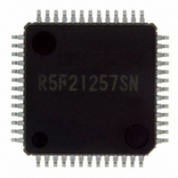
R5F21257SNFP#U0 Renesas Electronics America, R5F21257SNFP#U0 Datasheet - Page 214

R5F21257SNFP#U0
Manufacturer Part Number
R5F21257SNFP#U0
Description
IC R8C/25 MCU FLASH 52LQFP
Manufacturer
Renesas Electronics America
Series
R8C/2x/25r
Specifications of R5F21257SNFP#U0
Core Processor
R8C
Core Size
16/32-Bit
Speed
20MHz
Connectivity
I²C, LIN, SIO, SSU, UART/USART
Peripherals
POR, Voltage Detect, WDT
Number Of I /o
41
Program Memory Size
48KB (48K x 8)
Program Memory Type
FLASH
Ram Size
2.5K x 8
Voltage - Supply (vcc/vdd)
2.2 V ~ 5.5 V
Data Converters
A/D 12x10b
Oscillator Type
Internal
Operating Temperature
-20°C ~ 85°C
Package / Case
52-LQFP
For Use With
R0K521256S000BE - KIT EVAL STARTER FOR R8C/25
Lead Free Status / RoHS Status
Lead free / RoHS Compliant
Eeprom Size
-
Available stocks
Company
Part Number
Manufacturer
Quantity
Price
- Current page: 214 of 527
- Download datasheet (6Mb)
R8C/24 Group, R8C/25 Group
Rev.3.00
REJ09B0244-0300
Figure 14.45
TRDIOji input signal
14.3.5.1
fOCO40M
TRDCLK
Sampling clock
TRDIOji input signal
Input signal through
digital filtering
The TRDIOji input is sampled, and when the sampled input level matches 3 times, its level is determined.
Select the digital filter function and sampling clock by the TRDDFi register.
f32
f8
f4
f2
f1
Feb 29, 2008
= 011b
Timer RD operation clock
= 100b
= 010b
Digital Filter
Block Diagram of Digital Filter
i = 0 or 1, j = either A, B, C, or D
TCK0 to TCK2: Bits in TRDCRi register
DFCK0 to DFCK1 and DFj: Bits in TRDDF register
IOA0 to IOA2 and IOB0 to IOB2: Bits in TRDIORAi register
IOC0 to IOC3 and IOD0 to IOD3: Bits in TRDIORCi register
Clock period selected by
= 001b
bits TCK2 to TCK0 or
bits DFCK1 to DFCK0
= 101b
D
D
f1, fOCO40M)
= 000b
Latch
Latch
TCK2 to TCK0
C
C
Q
Q
= 110b
Page 195 of 485
Count source
D
f32
f8
f1
Latch
C
= 01b
= 10b
= 00b
= 11b
DFCK1 to DFCK0
Q
Transmission cannot be
performed without 3-time match
because the input signal is
assumed to be noise.
D
Latch
C
Sampling clock
Q
D
Latch
C
Q
detection
Match
circuit
Signal transmission delayed
up to 5-sampling clock
Recognition of the
signal change with
3-time match
1
0
DFj
Edge detection
IOC3 to IOC0
IOD3 to IOD0
IOA2 to IOA0
IOB2 to IOB0
circuit
14. Timers
Related parts for R5F21257SNFP#U0
Image
Part Number
Description
Manufacturer
Datasheet
Request
R

Part Number:
Description:
KIT STARTER FOR M16C/29
Manufacturer:
Renesas Electronics America
Datasheet:

Part Number:
Description:
KIT STARTER FOR R8C/2D
Manufacturer:
Renesas Electronics America
Datasheet:

Part Number:
Description:
R0K33062P STARTER KIT
Manufacturer:
Renesas Electronics America
Datasheet:

Part Number:
Description:
KIT STARTER FOR R8C/23 E8A
Manufacturer:
Renesas Electronics America
Datasheet:

Part Number:
Description:
KIT STARTER FOR R8C/25
Manufacturer:
Renesas Electronics America
Datasheet:

Part Number:
Description:
KIT STARTER H8S2456 SHARPE DSPLY
Manufacturer:
Renesas Electronics America
Datasheet:

Part Number:
Description:
KIT STARTER FOR R8C38C
Manufacturer:
Renesas Electronics America
Datasheet:

Part Number:
Description:
KIT STARTER FOR R8C35C
Manufacturer:
Renesas Electronics America
Datasheet:

Part Number:
Description:
KIT STARTER FOR R8CL3AC+LCD APPS
Manufacturer:
Renesas Electronics America
Datasheet:

Part Number:
Description:
KIT STARTER FOR RX610
Manufacturer:
Renesas Electronics America
Datasheet:

Part Number:
Description:
KIT STARTER FOR R32C/118
Manufacturer:
Renesas Electronics America
Datasheet:

Part Number:
Description:
KIT DEV RSK-R8C/26-29
Manufacturer:
Renesas Electronics America
Datasheet:

Part Number:
Description:
KIT STARTER FOR SH7124
Manufacturer:
Renesas Electronics America
Datasheet:

Part Number:
Description:
KIT STARTER FOR H8SX/1622
Manufacturer:
Renesas Electronics America
Datasheet:

Part Number:
Description:
KIT DEV FOR SH7203
Manufacturer:
Renesas Electronics America
Datasheet:


