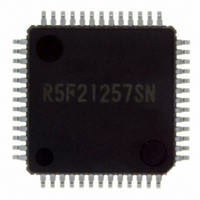
R5F21257SNFP#U0 Renesas Electronics America, R5F21257SNFP#U0 Datasheet - Page 334

R5F21257SNFP#U0
Manufacturer Part Number
R5F21257SNFP#U0
Description
IC R8C/25 MCU FLASH 52LQFP
Manufacturer
Renesas Electronics America
Series
R8C/2x/25r
Specifications of R5F21257SNFP#U0
Core Processor
R8C
Core Size
16/32-Bit
Speed
20MHz
Connectivity
I²C, LIN, SIO, SSU, UART/USART
Peripherals
POR, Voltage Detect, WDT
Number Of I /o
41
Program Memory Size
48KB (48K x 8)
Program Memory Type
FLASH
Ram Size
2.5K x 8
Voltage - Supply (vcc/vdd)
2.2 V ~ 5.5 V
Data Converters
A/D 12x10b
Oscillator Type
Internal
Operating Temperature
-20°C ~ 85°C
Package / Case
52-LQFP
For Use With
R0K521256S000BE - KIT EVAL STARTER FOR R8C/25
Lead Free Status / RoHS Status
Lead free / RoHS Compliant
Eeprom Size
-
Available stocks
Company
Part Number
Manufacturer
Quantity
Price
- Current page: 334 of 527
- Download datasheet (6Mb)
R8C/24 Group, R8C/25 Group
Rev.3.00
REJ09B0244-0300
16.2.1
16.2.1.1
The transfer clock can be selected from among seven internal clocks (f1/256, f1/128, f1/64, f1/32, f1/16, f1/8,
and f1/4) and an external clock.
When using clock synchronous serial I/O with chip select, set the SCKS bit in the SSMR2 register to 1 and
select the SSCK pin as the serial clock pin.
When the MSS bit in the SSCRH register is set to 1 (operates as master device), an internal clock can be
selected and the SSCK pin functions as output. When transfer is started, the SSCK pin outputs clocks of the
transfer rate selected by bits CKS0 to CKS2 in the SSCRH register.
When the MSS bit in the SSCRH register is set to 0 (operates as slave device), an external clock can be selected
and the SSCK pin functions as input.
The association between the transfer clock polarity, phase and data changes according to the combination of the
SSUMS bit in the SSMR2 register and bits CPHS and CPOS in the SSMR register.
Figure 16.10 shows the Association between Transfer Clock Polarity, Phase, and Transfer Data.
Also, the MSB-first transfer or LSB-first transfer can be selected by setting the MLS bit in the SSMR register.
When the MLS bit is set to 1, transfer is started from the LSB and proceeds to the MSB. When the MLS bit is
set to 0, transfer is started from the MSB and proceeds to the LSB.
Feb 29, 2008
Transfer Clock
Association between Transfer Clock Polarity, Phase, and Data
Page 315 of 485
16. Clock Synchronous Serial Interface
Related parts for R5F21257SNFP#U0
Image
Part Number
Description
Manufacturer
Datasheet
Request
R

Part Number:
Description:
KIT STARTER FOR M16C/29
Manufacturer:
Renesas Electronics America
Datasheet:

Part Number:
Description:
KIT STARTER FOR R8C/2D
Manufacturer:
Renesas Electronics America
Datasheet:

Part Number:
Description:
R0K33062P STARTER KIT
Manufacturer:
Renesas Electronics America
Datasheet:

Part Number:
Description:
KIT STARTER FOR R8C/23 E8A
Manufacturer:
Renesas Electronics America
Datasheet:

Part Number:
Description:
KIT STARTER FOR R8C/25
Manufacturer:
Renesas Electronics America
Datasheet:

Part Number:
Description:
KIT STARTER H8S2456 SHARPE DSPLY
Manufacturer:
Renesas Electronics America
Datasheet:

Part Number:
Description:
KIT STARTER FOR R8C38C
Manufacturer:
Renesas Electronics America
Datasheet:

Part Number:
Description:
KIT STARTER FOR R8C35C
Manufacturer:
Renesas Electronics America
Datasheet:

Part Number:
Description:
KIT STARTER FOR R8CL3AC+LCD APPS
Manufacturer:
Renesas Electronics America
Datasheet:

Part Number:
Description:
KIT STARTER FOR RX610
Manufacturer:
Renesas Electronics America
Datasheet:

Part Number:
Description:
KIT STARTER FOR R32C/118
Manufacturer:
Renesas Electronics America
Datasheet:

Part Number:
Description:
KIT DEV RSK-R8C/26-29
Manufacturer:
Renesas Electronics America
Datasheet:

Part Number:
Description:
KIT STARTER FOR SH7124
Manufacturer:
Renesas Electronics America
Datasheet:

Part Number:
Description:
KIT STARTER FOR H8SX/1622
Manufacturer:
Renesas Electronics America
Datasheet:

Part Number:
Description:
KIT DEV FOR SH7203
Manufacturer:
Renesas Electronics America
Datasheet:


