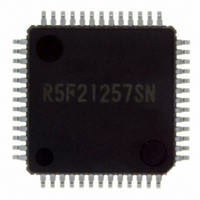
R5F21257SNFP#U0 Renesas Electronics America, R5F21257SNFP#U0 Datasheet - Page 506

R5F21257SNFP#U0
Manufacturer Part Number
R5F21257SNFP#U0
Description
IC R8C/25 MCU FLASH 52LQFP
Manufacturer
Renesas Electronics America
Series
R8C/2x/25r
Specifications of R5F21257SNFP#U0
Core Processor
R8C
Core Size
16/32-Bit
Speed
20MHz
Connectivity
I²C, LIN, SIO, SSU, UART/USART
Peripherals
POR, Voltage Detect, WDT
Number Of I /o
41
Program Memory Size
48KB (48K x 8)
Program Memory Type
FLASH
Ram Size
2.5K x 8
Voltage - Supply (vcc/vdd)
2.2 V ~ 5.5 V
Data Converters
A/D 12x10b
Oscillator Type
Internal
Operating Temperature
-20°C ~ 85°C
Package / Case
52-LQFP
For Use With
R0K521256S000BE - KIT EVAL STARTER FOR R8C/25
Lead Free Status / RoHS Status
Lead free / RoHS Compliant
Eeprom Size
-
Available stocks
Company
Part Number
Manufacturer
Quantity
Price
- Current page: 506 of 527
- Download datasheet (6Mb)
Rev.
0.20
REVISION HISTORY
Jan 16, 2006
Date
30 to 67
56 to 66
Page
27
28
33
34
46
47
49
50
51
67
69
71
72
73
75
77
78
79
80
81
82
5.2 Power-On Reset Function “When a capacitor is ... or more.” added
Figure 5.7 Example of Power-On Reset Circuit and Operation revised
5.4 Voltage Monitor 1 Reset;
“6. Programmable I/O Ports” → “6. Voltage Detection Circuit” and
“7. Voltage Detection Circuit” → “7. Programmable I/O Ports” revised
Figure 6.5 Registers VCA1 and VCA2; VCA2 register revised
Figure 6.6 VW0C Register revised
Figure 7.2 Configuration of Programmable I/O Ports (2) revised
Figure 7.3 Configuration of Programmable I/O Ports (3) revised
Figure 7.5 Configuration of Programmable I/O Ports (5) revised
Figure 7.6 Configuration of Programmable I/O Ports (6) revised
Figure 7.7 Configuration of Programmable I/O Ports (7) revised
7.4 Port setting added;
Table 7.48 Unassigned Pin Handling revised
9. Bus revised;
Table 9.2 Bus Cycles by Access Space of the R8C/25 Group added,
Table 9.3 Access Unit and Bus Operations;
Figure 10.1 Clock Generation Circuit revised
Figure 10.2 CM0 Register revised
Figure 10.3 CM1 Register revised
Figure 10.5 Registers FRA0 and FRA1; FRA0 register revised
Figure 10.8 VCA2 Register added
Figure 10.9 Examples of XIN Clock Connection Circuit revised
10.2.2 High-Speed On-Chip Oscillator Clock;
10.3 XCIN Clock “To input an external clock ... pin open.” added
10.4.2 CPU Clock “Use the XCIN clock while ... stabilizes.” added
10.4.3 Peripheral Function Clock (f1, f2, f4, f8, f32, fC4, and fC32);
10.4.5 fOCO40M;
10.4.8 fOCO128 added
Table 10.2 Settings and Modes of Clock Associated Bits revised
R8C/24 Group, R8C/25 Group Hardware Manual
“When ... VCC pin drops the Vdet1 ...” → “When ... VCC pin reaches to
the Vdet1 ...” revised
Table 7.4 Port P0_0/AN7 to Table 7.47 Port P6_7/INT3/RXD1 added
“However, only following SFRs are ... accessed at a time.” added
“SFR” → “SFR, data flash”,
“ROM/RAM” → “ROM (program ROM), RAM” revised
“To use the high-speed on-chip ... or more).” added
“Use fC4 and fC32 while the XCIN clock oscillation stabilizes.” added
“fOCO40M can be ... supply voltage VCC = 3.0 to 5.5 V.” added
C - 2
Description
Summary
Related parts for R5F21257SNFP#U0
Image
Part Number
Description
Manufacturer
Datasheet
Request
R

Part Number:
Description:
KIT STARTER FOR M16C/29
Manufacturer:
Renesas Electronics America
Datasheet:

Part Number:
Description:
KIT STARTER FOR R8C/2D
Manufacturer:
Renesas Electronics America
Datasheet:

Part Number:
Description:
R0K33062P STARTER KIT
Manufacturer:
Renesas Electronics America
Datasheet:

Part Number:
Description:
KIT STARTER FOR R8C/23 E8A
Manufacturer:
Renesas Electronics America
Datasheet:

Part Number:
Description:
KIT STARTER FOR R8C/25
Manufacturer:
Renesas Electronics America
Datasheet:

Part Number:
Description:
KIT STARTER H8S2456 SHARPE DSPLY
Manufacturer:
Renesas Electronics America
Datasheet:

Part Number:
Description:
KIT STARTER FOR R8C38C
Manufacturer:
Renesas Electronics America
Datasheet:

Part Number:
Description:
KIT STARTER FOR R8C35C
Manufacturer:
Renesas Electronics America
Datasheet:

Part Number:
Description:
KIT STARTER FOR R8CL3AC+LCD APPS
Manufacturer:
Renesas Electronics America
Datasheet:

Part Number:
Description:
KIT STARTER FOR RX610
Manufacturer:
Renesas Electronics America
Datasheet:

Part Number:
Description:
KIT STARTER FOR R32C/118
Manufacturer:
Renesas Electronics America
Datasheet:

Part Number:
Description:
KIT DEV RSK-R8C/26-29
Manufacturer:
Renesas Electronics America
Datasheet:

Part Number:
Description:
KIT STARTER FOR SH7124
Manufacturer:
Renesas Electronics America
Datasheet:

Part Number:
Description:
KIT STARTER FOR H8SX/1622
Manufacturer:
Renesas Electronics America
Datasheet:

Part Number:
Description:
KIT DEV FOR SH7203
Manufacturer:
Renesas Electronics America
Datasheet:


