R5F21257SNFP#U0 Renesas Electronics America, R5F21257SNFP#U0 Datasheet - Page 344
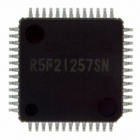
R5F21257SNFP#U0
Manufacturer Part Number
R5F21257SNFP#U0
Description
IC R8C/25 MCU FLASH 52LQFP
Manufacturer
Renesas Electronics America
Series
R8C/2x/25r
Specifications of R5F21257SNFP#U0
Core Processor
R8C
Core Size
16/32-Bit
Speed
20MHz
Connectivity
I²C, LIN, SIO, SSU, UART/USART
Peripherals
POR, Voltage Detect, WDT
Number Of I /o
41
Program Memory Size
48KB (48K x 8)
Program Memory Type
FLASH
Ram Size
2.5K x 8
Voltage - Supply (vcc/vdd)
2.2 V ~ 5.5 V
Data Converters
A/D 12x10b
Oscillator Type
Internal
Operating Temperature
-20°C ~ 85°C
Package / Case
52-LQFP
For Use With
R0K521256S000BE - KIT EVAL STARTER FOR R8C/25
Lead Free Status / RoHS Status
Lead free / RoHS Compliant
Eeprom Size
-
Available stocks
Company
Part Number
Manufacturer
Quantity
Price


R8C/24 Group, R8C/25 Group
Rev.3.00
REJ09B0244-0300
16.2.5.4
Data transmission/reception is an operation combining data transmission and reception which were described
earlier. Transmission/reception is started by writing data to the SSTDR register.
When the 8th clock rises or the ORER bit is set to 1 (overrun error) while the TDRE bit is set to 1 (data is
transferred from registers SSTDR to SSTRSR), the transmit/receive operation is stopped.
When switching from transmit mode (TE = 1) or receive mode (RE = 1) to transmit/receive mode (Te = RE =
1), set the TE bit to 0 and RE bit to 0 before switching. After confirming that the TEND bit is set to 0 (the
TDRE bit is set to 0 when the last bit of the transmit data is transmitted), the RDRF bit is set to 0 (no data in the
SSRDR register), and the ORER bit is set to 0 (no overrun error), set bits TE and RE to 1.
Figure 16.17 shows a Sample Flowchart of Data Transmission/Reception (Clock Synchronous Communication
Mode).
Feb 29, 2008
Data Transmission/Reception
Page 325 of 485
16. Clock Synchronous Serial Interface
Related parts for R5F21257SNFP#U0
Image
Part Number
Description
Manufacturer
Datasheet
Request
R

Part Number:
Description:
KIT STARTER FOR M16C/29
Manufacturer:
Renesas Electronics America
Datasheet:

Part Number:
Description:
KIT STARTER FOR R8C/2D
Manufacturer:
Renesas Electronics America
Datasheet:

Part Number:
Description:
R0K33062P STARTER KIT
Manufacturer:
Renesas Electronics America
Datasheet:

Part Number:
Description:
KIT STARTER FOR R8C/23 E8A
Manufacturer:
Renesas Electronics America
Datasheet:

Part Number:
Description:
KIT STARTER FOR R8C/25
Manufacturer:
Renesas Electronics America
Datasheet:

Part Number:
Description:
KIT STARTER H8S2456 SHARPE DSPLY
Manufacturer:
Renesas Electronics America
Datasheet:

Part Number:
Description:
KIT STARTER FOR R8C38C
Manufacturer:
Renesas Electronics America
Datasheet:

Part Number:
Description:
KIT STARTER FOR R8C35C
Manufacturer:
Renesas Electronics America
Datasheet:

Part Number:
Description:
KIT STARTER FOR R8CL3AC+LCD APPS
Manufacturer:
Renesas Electronics America
Datasheet:
Part Number:
Description:
KIT STARTER FOR RX610
Manufacturer:
Renesas Electronics America
Datasheet:

Part Number:
Description:
KIT STARTER FOR R32C/118
Manufacturer:
Renesas Electronics America
Datasheet:

Part Number:
Description:
KIT DEV RSK-R8C/26-29
Manufacturer:
Renesas Electronics America
Datasheet:

Part Number:
Description:
KIT STARTER FOR SH7124
Manufacturer:
Renesas Electronics America
Datasheet:

Part Number:
Description:
KIT STARTER FOR H8SX/1622
Manufacturer:
Renesas Electronics America
Datasheet:

Part Number:
Description:
KIT DEV FOR SH7203
Manufacturer:
Renesas Electronics America
Datasheet: