R5F21257SNFP#U0 Renesas Electronics America, R5F21257SNFP#U0 Datasheet - Page 210
R5F21257SNFP#U0
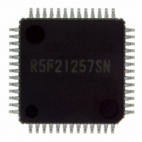
Manufacturer Part Number
R5F21257SNFP#U0
Description
IC R8C/25 MCU FLASH 52LQFP
Manufacturer
Renesas Electronics America
Series
R8C/2x/25r
Specifications of R5F21257SNFP#U0
Core Processor
R8C
Core Size
16/32-Bit
Speed
20MHz
Connectivity
I²C, LIN, SIO, SSU, UART/USART
Peripherals
POR, Voltage Detect, WDT
Number Of I /o
41
Program Memory Size
48KB (48K x 8)
Program Memory Type
FLASH
Ram Size
2.5K x 8
Voltage - Supply (vcc/vdd)
2.2 V ~ 5.5 V
Data Converters
A/D 12x10b
Oscillator Type
Internal
Operating Temperature
-20°C ~ 85°C
Package / Case
52-LQFP
For Use With
R0K521256S000BE - KIT EVAL STARTER FOR R8C/25
Lead Free Status / RoHS Status
Lead free / RoHS Compliant
Eeprom Size
-
Available stocks
Company
Part Number
Manufacturer
Quantity
Price


R8C/24 Group, R8C/25 Group
Rev.3.00
REJ09B0244-0300
Figure 14.40
Timer RD Status Register i (i = 0 or 1)
b7 b6 b5 b4
NOTES:
1.
2.
3.
4. Edge selected by bits IOk1 to IOk0 (k = C or D) in the TRDIORCi register
Nothing is assigned to b5 in the TRDSR0 register. When w riting to b5, w rite 0. When reading, the content is 1.
The w riting results are as follow s:
• This bit is set to 0 w hen the read result is 1 and 0 is w ritten to the same bit.
• This bit remains unchanged even if the read result is 0 and 0 is w ritten to the same bit. (This bit remains 1 even
• This bit remains unchanged if 1 is w ritten to it.
Edge selected by bits IOj1 to IOj0 (j = A or B) in the TRDIORAi register.
Including w hen the BFki bit in the TRDMR register is set to 1 (TRDGRki is used as the buffer register).
Feb 29, 2008
if it is set to 1 from 0 after reading, and w riting 0.)
b3 b2
Registers TRDSR0 to TRDSR1 in Input Capture Function
b1 b0
Bit Symbol
TRDSR0
TRDSR1
(b7-b6)
Symbol
IMFA
IMFB
IMFC
IMFD
OVF
UDF
Page 191 of 485
—
Input capture/compare match
flag A
Input capture/compare match
flag B
Input capture/compare match
flag C
Input capture/compare match
flag D
Overflow flag
Underflow flag
Nothing is assigned. If necessary, set to 0.
When read, the content is 1.
Address
Bit Name
0143h
0153h
(1)
[Source for setting this bit to 0]
Write 0 after read
[Source for setting this bit to 1]
TRDSR0 register:
fOCO128 signal edge w hen the IOA3 bit in the
TRDIORA0 register is set to 0 (fOCO128 signal)
TRDIOA0 pin input edge w hen the IOA3 bit in the
TRDIORA0 register is set to 1 (TRDIOA0 input)
TRDSR1 register:
Input edge of TRDIOA1 pin
[Source for setting this bit to 0]
Write 0 after read
[Source for setting this bit to 1]
Input edge of TRDIOBi pin
[Source for setting this bit to 0]
Write 0 after read
[Source for setting this bit to 1]
Input edge of TRDIOCi pin
[Source for setting this bit to 0]
Write 0 after read
[Source for setting this bit to 1]
Input edge of TRDIODi pin
[Source for setting this bit to 0]
Write 0 after read
[Source for setting this bit to 1]
When the TRDi register overflow s
This bit is disabled in the input capture function.
(2)
(2)
(2)
(2)
(2)
After Reset
11100000b
11000000b
Function
(3)
(4)
(4)
(3)
(3)
14. Timers
RW
RW
RW
RW
RW
RW
RW
—
Related parts for R5F21257SNFP#U0
Image
Part Number
Description
Manufacturer
Datasheet
Request
R

Part Number:
Description:
KIT STARTER FOR M16C/29
Manufacturer:
Renesas Electronics America
Datasheet:

Part Number:
Description:
KIT STARTER FOR R8C/2D
Manufacturer:
Renesas Electronics America
Datasheet:

Part Number:
Description:
R0K33062P STARTER KIT
Manufacturer:
Renesas Electronics America
Datasheet:

Part Number:
Description:
KIT STARTER FOR R8C/23 E8A
Manufacturer:
Renesas Electronics America
Datasheet:

Part Number:
Description:
KIT STARTER FOR R8C/25
Manufacturer:
Renesas Electronics America
Datasheet:

Part Number:
Description:
KIT STARTER H8S2456 SHARPE DSPLY
Manufacturer:
Renesas Electronics America
Datasheet:

Part Number:
Description:
KIT STARTER FOR R8C38C
Manufacturer:
Renesas Electronics America
Datasheet:

Part Number:
Description:
KIT STARTER FOR R8C35C
Manufacturer:
Renesas Electronics America
Datasheet:

Part Number:
Description:
KIT STARTER FOR R8CL3AC+LCD APPS
Manufacturer:
Renesas Electronics America
Datasheet:
Part Number:
Description:
KIT STARTER FOR RX610
Manufacturer:
Renesas Electronics America
Datasheet:

Part Number:
Description:
KIT STARTER FOR R32C/118
Manufacturer:
Renesas Electronics America
Datasheet:

Part Number:
Description:
KIT DEV RSK-R8C/26-29
Manufacturer:
Renesas Electronics America
Datasheet:

Part Number:
Description:
KIT STARTER FOR SH7124
Manufacturer:
Renesas Electronics America
Datasheet:

Part Number:
Description:
KIT STARTER FOR H8SX/1622
Manufacturer:
Renesas Electronics America
Datasheet:

Part Number:
Description:
KIT DEV FOR SH7203
Manufacturer:
Renesas Electronics America
Datasheet: