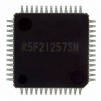
R5F21257SNFP#U0 Renesas Electronics America, R5F21257SNFP#U0 Datasheet - Page 518

R5F21257SNFP#U0
Manufacturer Part Number
R5F21257SNFP#U0
Description
IC R8C/25 MCU FLASH 52LQFP
Manufacturer
Renesas Electronics America
Series
R8C/2x/25r
Specifications of R5F21257SNFP#U0
Core Processor
R8C
Core Size
16/32-Bit
Speed
20MHz
Connectivity
I²C, LIN, SIO, SSU, UART/USART
Peripherals
POR, Voltage Detect, WDT
Number Of I /o
41
Program Memory Size
48KB (48K x 8)
Program Memory Type
FLASH
Ram Size
2.5K x 8
Voltage - Supply (vcc/vdd)
2.2 V ~ 5.5 V
Data Converters
A/D 12x10b
Oscillator Type
Internal
Operating Temperature
-20°C ~ 85°C
Package / Case
52-LQFP
For Use With
R0K521256S000BE - KIT EVAL STARTER FOR R8C/25
Lead Free Status / RoHS Status
Lead free / RoHS Compliant
Eeprom Size
-
Available stocks
Company
Part Number
Manufacturer
Quantity
Price
- Current page: 518 of 527
- Download datasheet (6Mb)
Rev.
1.00
REVISION HISTORY
May 31, 2006
Date
Page
372
373
374
376
380
384
386
387
388
389
394
395
397
399
401
402
405
406
407
408
409
410
413
414
Figure 17.10 Example of Header Field Reception Flowchart (3) revised
Figure 17.11 Typical Operation when a Bus Collision is Detected;
17.5 Interrupt Requests;
18.6 Inflow Current Bypass Circuit deleted
19.4.2.1 FMR00 Bit
Table 17.2 Interrupt Requests of Hardware LIN revised
Table 18.1 Performance of A/D converter revised
Table 18.2 One-Shot Mode Specifications revised
Figure 18.6 ADCON0 Register in Repeat Mode revised
18.3 Sample and Hold;
Figure 18.10 Internal Equivalent Circuit of Analog Input revised
18.6 Output Impedance of Sensor under A/D Conversion added
18.7 Notes on A/D Converter revised
Figure 19.4 OFS Register NOTE2 revised
Table 19.3 Differences between EW0 Mode and EW1 Mode revised
Figure 19.5 FMR0 Register NOTE6 added
Figure 19.7 FMR4 Register; NOTES 2, 3 and 4 revised and NOTE5 added
Figure 19.8 Timing of Suspend Operation revised
19.4.3.1 Read Array Command
19.4.3.2 Read Status Register Command
19.4.3.4 Program Command;
Figure 19.12 Program Command (When Suspend Function Disabled) title revised
Figure 19.13 Program Command (When Suspend Function Enabled) added
19.4.3.5 Block Erase revised
Figure 19.14 Block Erase Command (When Erase-Suspend Function
Disabled) title revised
Figure 19.15 Block Erase Command (When Erase-Suspend Function
Enabled) revised
Table 19.5 Status Register Bits revised
19.5 Standard Serial I/O Mode revised
Table 19.7 Pin Functions (Flash Memory Standard Serial I/O Mode 2) added
Table 19.8 Pin Functions (Flash Memory Standard Serial I/O Mode 3) revised
R8C/24 Group, R8C/25 Group Hardware Manual
“RAIC” → “TRAIC” revised
“There are four ... Sync Break generation completed, ... , and bus collision
detection.” → “There are three ... , and bus collision detection.” revised
“... to 28 φ AD cycles for 8-bit resolution or 33 φ AD resolution” and
“When performing A/D conversion, charge the sampling time.” deleted
“... (including suspend periods) ...” added
“The MCU also enters read array mode after a reset.” added
“The MCU remains in read status mode ... command is written.” added
“When suspend function disabled, ...”, “When suspend function
enabled, the FMR44 bit ... when auto-programming completes.” added
C - 14
Description
Summary
Related parts for R5F21257SNFP#U0
Image
Part Number
Description
Manufacturer
Datasheet
Request
R

Part Number:
Description:
KIT STARTER FOR M16C/29
Manufacturer:
Renesas Electronics America
Datasheet:

Part Number:
Description:
KIT STARTER FOR R8C/2D
Manufacturer:
Renesas Electronics America
Datasheet:

Part Number:
Description:
R0K33062P STARTER KIT
Manufacturer:
Renesas Electronics America
Datasheet:

Part Number:
Description:
KIT STARTER FOR R8C/23 E8A
Manufacturer:
Renesas Electronics America
Datasheet:

Part Number:
Description:
KIT STARTER FOR R8C/25
Manufacturer:
Renesas Electronics America
Datasheet:

Part Number:
Description:
KIT STARTER H8S2456 SHARPE DSPLY
Manufacturer:
Renesas Electronics America
Datasheet:

Part Number:
Description:
KIT STARTER FOR R8C38C
Manufacturer:
Renesas Electronics America
Datasheet:

Part Number:
Description:
KIT STARTER FOR R8C35C
Manufacturer:
Renesas Electronics America
Datasheet:

Part Number:
Description:
KIT STARTER FOR R8CL3AC+LCD APPS
Manufacturer:
Renesas Electronics America
Datasheet:

Part Number:
Description:
KIT STARTER FOR RX610
Manufacturer:
Renesas Electronics America
Datasheet:

Part Number:
Description:
KIT STARTER FOR R32C/118
Manufacturer:
Renesas Electronics America
Datasheet:

Part Number:
Description:
KIT DEV RSK-R8C/26-29
Manufacturer:
Renesas Electronics America
Datasheet:

Part Number:
Description:
KIT STARTER FOR SH7124
Manufacturer:
Renesas Electronics America
Datasheet:

Part Number:
Description:
KIT STARTER FOR H8SX/1622
Manufacturer:
Renesas Electronics America
Datasheet:

Part Number:
Description:
KIT DEV FOR SH7203
Manufacturer:
Renesas Electronics America
Datasheet:


