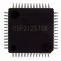
R5F21257SNFP#U0 Renesas Electronics America, R5F21257SNFP#U0 Datasheet - Page 201

R5F21257SNFP#U0
Manufacturer Part Number
R5F21257SNFP#U0
Description
IC R8C/25 MCU FLASH 52LQFP
Manufacturer
Renesas Electronics America
Series
R8C/2x/25r
Specifications of R5F21257SNFP#U0
Core Processor
R8C
Core Size
16/32-Bit
Speed
20MHz
Connectivity
I²C, LIN, SIO, SSU, UART/USART
Peripherals
POR, Voltage Detect, WDT
Number Of I /o
41
Program Memory Size
48KB (48K x 8)
Program Memory Type
FLASH
Ram Size
2.5K x 8
Voltage - Supply (vcc/vdd)
2.2 V ~ 5.5 V
Data Converters
A/D 12x10b
Oscillator Type
Internal
Operating Temperature
-20°C ~ 85°C
Package / Case
52-LQFP
For Use With
R0K521256S000BE - KIT EVAL STARTER FOR R8C/25
Lead Free Status / RoHS Status
Lead free / RoHS Compliant
Eeprom Size
-
Available stocks
Company
Part Number
Manufacturer
Quantity
Price
- Current page: 201 of 527
- Download datasheet (6Mb)
R8C/24 Group, R8C/25 Group
Rev.3.00
REJ09B0244-0300
Figure 14.32
14.3.5
i = 0 or 1
NOTE 1: When the BFCi bit in the TRDMR register is set to 1 (the TRDGRCi register is used as the buffer register of the
NOTE 2: When the BFDi bit in the TRDMR register is set to 1 (the TRDGRDi register is used as the buffer register of the
TRDIOAi
TRDIOCi
TRDIOBi
TRDIODi
The input capture function measures the external signal width and period. The content of the TRDi register
(counter) is transferred to the TRDGRji register as a trigger of the TRDIOji (i = 0 or 1, j = either A, B, C, or D)
pin external signal (input capture). Since this function is enabled with a combination of the TRDIOji pin and
TRDGRji register, the input capture function, or any other mode or function, can be selected for each individual
pin.
The TRDGRA0 register can also select fOCO128 signal as input-capture trigger input.
Figure 14.32 shows a Block Diagram of Input Capture Function, Table 14.23 lists the Input Capture Function
Specifications. Figures 14.33 to 14.43 show the Registers Associated with Input Capture Function, and Figure
14.44 shows an Operating Example of Input Capture Function.
TRDGRAi register).
TRDGRBi register).
Feb 29, 2008
(3)
Input Capture Function
Block Diagram of Input Capture Function
(Note 1)
(Note 2)
Page 182 of 485
Input capture
signal
Input capture
signal
Input capture
signal
Input capture
signal
TRDGRAi
TRDGRCi
TRDGRBi
TRDGRDi
register
register
register
register
TRDi register
TRDIOA0
NOTE 3: The trigger input of the TRDGRA0 register
fOCO
can select the TRDIOA0 pin input or
fOCO128 signal.
Divided
by 128
fOCO128
IOA3 = 0
IOA3 = 1
Input capture
signal
14. Timers
Related parts for R5F21257SNFP#U0
Image
Part Number
Description
Manufacturer
Datasheet
Request
R

Part Number:
Description:
KIT STARTER FOR M16C/29
Manufacturer:
Renesas Electronics America
Datasheet:

Part Number:
Description:
KIT STARTER FOR R8C/2D
Manufacturer:
Renesas Electronics America
Datasheet:

Part Number:
Description:
R0K33062P STARTER KIT
Manufacturer:
Renesas Electronics America
Datasheet:

Part Number:
Description:
KIT STARTER FOR R8C/23 E8A
Manufacturer:
Renesas Electronics America
Datasheet:

Part Number:
Description:
KIT STARTER FOR R8C/25
Manufacturer:
Renesas Electronics America
Datasheet:

Part Number:
Description:
KIT STARTER H8S2456 SHARPE DSPLY
Manufacturer:
Renesas Electronics America
Datasheet:

Part Number:
Description:
KIT STARTER FOR R8C38C
Manufacturer:
Renesas Electronics America
Datasheet:

Part Number:
Description:
KIT STARTER FOR R8C35C
Manufacturer:
Renesas Electronics America
Datasheet:

Part Number:
Description:
KIT STARTER FOR R8CL3AC+LCD APPS
Manufacturer:
Renesas Electronics America
Datasheet:

Part Number:
Description:
KIT STARTER FOR RX610
Manufacturer:
Renesas Electronics America
Datasheet:

Part Number:
Description:
KIT STARTER FOR R32C/118
Manufacturer:
Renesas Electronics America
Datasheet:

Part Number:
Description:
KIT DEV RSK-R8C/26-29
Manufacturer:
Renesas Electronics America
Datasheet:

Part Number:
Description:
KIT STARTER FOR SH7124
Manufacturer:
Renesas Electronics America
Datasheet:

Part Number:
Description:
KIT STARTER FOR H8SX/1622
Manufacturer:
Renesas Electronics America
Datasheet:

Part Number:
Description:
KIT DEV FOR SH7203
Manufacturer:
Renesas Electronics America
Datasheet:


