M38039FFHFP#U0 Renesas Electronics America, M38039FFHFP#U0 Datasheet - Page 108
M38039FFHFP#U0
Manufacturer Part Number
M38039FFHFP#U0
Description
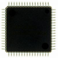
IC 740 MCU FLASH 60K 64QFP
Manufacturer
Renesas Electronics America
Series
740/38000r
Datasheet
1.M38039FFHFPU0.pdf
(119 pages)
Specifications of M38039FFHFP#U0
Core Processor
740
Core Size
8-Bit
Speed
16.8MHz
Connectivity
SIO, UART/USART
Peripherals
PWM, WDT
Number Of I /o
56
Program Memory Size
60KB (60K x 8)
Program Memory Type
FLASH
Ram Size
2K x 8
Voltage - Supply (vcc/vdd)
2.7 V ~ 5.5 V
Data Converters
A/D 16x10b; D/A 2x8b
Oscillator Type
Internal
Operating Temperature
-20°C ~ 85°C
Package / Case
64-QFP
Lead Free Status / RoHS Status
Lead free / RoHS Compliant
Eeprom Size
-
Available stocks
Company
Part Number
Manufacturer
Quantity
Price


3803 Group (Spec.H)
Rev.3.11
REJ03B0017-0311
NOTES
NOTES ON PROGRAMMING
1. Processor Status Register
(1) Initializing of processor status register
Flags which affect program execution must be initialized after a reset.
In particular, it is essential to initialize the T and D flags because
they have an important effect on calculations.
<Reason>
After a reset, the contents of the processor status register (PS) are
undefined except for the I flag which is “1”.
Fig 85. Initialization of processor status register
(2) How to reference the processor status register
To reference the contents of the processor status register (PS),
execute the PHP instruction once then read the contents of (S+1).
If necessary, execute the PLP instruction to return the PS to its
original status.
Fig 86. Stack memory contents after PHP instruction
2. BRK instruction
(1) Interrupt priority level
When the BRK instruction is executed with the following
conditions satisfied, the interrupt execution is started from the
address of interrupt vector which has the highest priority.
• Interrupt request bit and interrupt enable bit are set to “1”.
• Interrupt disable flag (I) is set to “1” to disable interrupt.
3. Decimal calculations
(1) Execution of decimal calculations
The ADC and SBC are the only instructions which will yield
proper decimal notation, set the decimal mode flag (D) to “1”
with the SED instruction. After executing the ADC or SBC
instruction, execute another instruction before executing the
SEC, CLC, or CLD instruction.
(2) Notes on status flag in decimal mode
When decimal mode is selected, the values of three of the flags in
the status register (the N, V, and Z flags) are invalid after a ADC
or SBC instruction is executed.
The carry flag (C) is set to “1” if a carry is generated as a result of the
calculation, or is cleared to “0” if a borrow is generated. To
determine whether a calculation has generated a carry, the C flag
must be initialized to “0” before each calculation. To check for a
borrow, the C flag must be initialized to “1” before each calculation.
execution
Apr 5, 2006
(S) + 1
(S)
Initializing of flags
Main program
Reset
Stored PS
Page 106 of 113
Fig 87. Execution of decimal calculations
4. JMP instruction
When using the JMP instruction in indirect addressing mode, do
not specify the last address on a page as an indirect address.
5. Multiplication and Division Instructions
• The index X mode (T) and the decimal mode (D) flags do not
• The execution of these instructions does not change the
6. Ports
The contents of the port direction registers cannot be read. The
following cannot be used:
• The data transfer instruction (LDA, etc.)
• The operation instruction when the index X mode flag (T) is “1”
• The instruction with the addressing mode which uses the value
• The bit-test instruction (BBC or BBS, etc.) to a direction
• The read-modify-write instructions (ROR, CLB, or SEB, etc.)
Use instructions such as LDM and STA, etc., to set the port
direction registers.
7. Instruction Execution Timing
The instruction execution time can be obtained by multiplying
the frequency of the internal clock
mentioned in the 740 Family Software Manual.
The frequency of the internal clock
high-speed mode, 8 times the X
and the twice the X
affect the MUL and DIV instruction.
contents of the processor status register.
of a direction register as an index
register
to a direction register.
SEC, CLC, or CLD instruction
CIN
ADC or SBC instruction
in low-speed mode.
Set D flag to “1”
NOP instruction
IN
φ
cycle in middle-speed mode,
is the twice the X
φ
by the number of cycles
IN
cycle in
Related parts for M38039FFHFP#U0
Image
Part Number
Description
Manufacturer
Datasheet
Request
R

Part Number:
Description:
KIT STARTER FOR M16C/29
Manufacturer:
Renesas Electronics America
Datasheet:

Part Number:
Description:
KIT STARTER FOR R8C/2D
Manufacturer:
Renesas Electronics America
Datasheet:

Part Number:
Description:
R0K33062P STARTER KIT
Manufacturer:
Renesas Electronics America
Datasheet:

Part Number:
Description:
KIT STARTER FOR R8C/23 E8A
Manufacturer:
Renesas Electronics America
Datasheet:

Part Number:
Description:
KIT STARTER FOR R8C/25
Manufacturer:
Renesas Electronics America
Datasheet:

Part Number:
Description:
KIT STARTER H8S2456 SHARPE DSPLY
Manufacturer:
Renesas Electronics America
Datasheet:

Part Number:
Description:
KIT STARTER FOR R8C38C
Manufacturer:
Renesas Electronics America
Datasheet:

Part Number:
Description:
KIT STARTER FOR R8C35C
Manufacturer:
Renesas Electronics America
Datasheet:

Part Number:
Description:
KIT STARTER FOR R8CL3AC+LCD APPS
Manufacturer:
Renesas Electronics America
Datasheet:
Part Number:
Description:
KIT STARTER FOR RX610
Manufacturer:
Renesas Electronics America
Datasheet:

Part Number:
Description:
KIT STARTER FOR R32C/118
Manufacturer:
Renesas Electronics America
Datasheet:

Part Number:
Description:
KIT DEV RSK-R8C/26-29
Manufacturer:
Renesas Electronics America
Datasheet:

Part Number:
Description:
KIT STARTER FOR SH7124
Manufacturer:
Renesas Electronics America
Datasheet:

Part Number:
Description:
KIT STARTER FOR H8SX/1622
Manufacturer:
Renesas Electronics America
Datasheet:

Part Number:
Description:
KIT DEV FOR SH7203
Manufacturer:
Renesas Electronics America
Datasheet: