M38039FFHFP#U0 Renesas Electronics America, M38039FFHFP#U0 Datasheet - Page 118
M38039FFHFP#U0
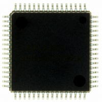
Manufacturer Part Number
M38039FFHFP#U0
Description
IC 740 MCU FLASH 60K 64QFP
Manufacturer
Renesas Electronics America
Series
740/38000r
Datasheet
1.M38039FFHFPU0.pdf
(119 pages)
Specifications of M38039FFHFP#U0
Core Processor
740
Core Size
8-Bit
Speed
16.8MHz
Connectivity
SIO, UART/USART
Peripherals
PWM, WDT
Number Of I /o
56
Program Memory Size
60KB (60K x 8)
Program Memory Type
FLASH
Ram Size
2K x 8
Voltage - Supply (vcc/vdd)
2.7 V ~ 5.5 V
Data Converters
A/D 16x10b; D/A 2x8b
Oscillator Type
Internal
Operating Temperature
-20°C ~ 85°C
Package / Case
64-QFP
Lead Free Status / RoHS Status
Lead free / RoHS Compliant
Eeprom Size
-
Available stocks
Company
Part Number
Manufacturer
Quantity
Price


Rev.
3.03
3.10
3.11
REVISION HISTORY
Nov.14, 2005
Jun.17, 2005
Apr.5, 2006
Date
106 to 108 PACKAGE OUTLINE revised.
106 to 108 PACKAGE OUTLINE revised.
109 to 116 Appendix added.
74 to 85
44, 52
86, 87
96, 97
Page
1, 5
89
20
61
88
13
15
17
19
56
57
64
5
9
7
9
-
Fig.3, Table 5 Package name revised.
“Packages” Package name revised.
Fig.74 to Fig.77 Package name revised.
Table 17 is partly revised.
Bit name revised: STP instruction disable bit
bit
Fig.15 Port block diagram (18) Port P56 revised.
Watchdog Timer Operations revised.
Bit 6 of Watchdog Timer Control Register added.
Fig.55: Block diagram of Watchdog timer revised.
Fig.56: Structure of Watchdog timer control register revised.
Flash Memory Version revised.
Fig.80: Wiring for the CNVSS pin added.
Table 1, Table 5, Fig.3; M38037M8H-XXXWG deleted.
Table 6 Functions revised.
Packages; “LGA”
[CPU Mode Register (CPUM)] “The CPU mode register .... selection bit, etc.”
“The CPU mode register ....selection bit, the internal system clock control bits, etc.”
MEMORY <Note> added.
I/O PORTS; “By setting the port P0 pull-up control register....programmed as the
output ports.” added.
Table 9 Input/Output added.
Fig.14 Port P4
[Serial I/O1 Status Register (SIO1STS)] “If there is an error,....the transmit buffer
empty flag (bit 0) become “1”.” revised.
•Data Setting “count source selection bit = “0”” added.
Fig.47 “X
Fig.48; “f(X
Frequency Control; (4) Low power dissipation mode added.
Oscillation Control; (2) Wait mode, <Notes> added.
Fig.78, Fig.79 added.
NOTES ON PROGRAMMING, NOTES ON USAGE deleted.
→
Table 24, Table 27; f(X
Bit name and its description revised. (Bit function is not changed.)
→ STP instruction function selection bit
0 : Entering stop mode by execution of STP instruction
1 : Internal reset by execution of STP instruction
Conditions: “V
Limits Max.:
Included in NOTES
<Notes> added.
IN
CIN
or X
“
) at low-speed mode”
0
(
-----------------------------------------------------------
CC
, P4
24
CIN
”
→
×
”
→
1
V
→
“FLGA”
3803 Group (Spec.H) Data Sheet
revised.
(3/3)
CC
“V
IN
“X
CC
)
–
3
IN
60
= V
(X
)
×
CIN
Description
REF
1.05
at low-speed mode)
”
”
,
→
“f(X
Summary
“
(
---------------------------------------------------------------------
CIN
24.6
)/2 at low-speed mode” added.
→
×
V
STP instruction function selection
C C
–
3
62.7
)
×
1.05
”
→
Related parts for M38039FFHFP#U0
Image
Part Number
Description
Manufacturer
Datasheet
Request
R

Part Number:
Description:
KIT STARTER FOR M16C/29
Manufacturer:
Renesas Electronics America
Datasheet:

Part Number:
Description:
KIT STARTER FOR R8C/2D
Manufacturer:
Renesas Electronics America
Datasheet:

Part Number:
Description:
R0K33062P STARTER KIT
Manufacturer:
Renesas Electronics America
Datasheet:

Part Number:
Description:
KIT STARTER FOR R8C/23 E8A
Manufacturer:
Renesas Electronics America
Datasheet:

Part Number:
Description:
KIT STARTER FOR R8C/25
Manufacturer:
Renesas Electronics America
Datasheet:

Part Number:
Description:
KIT STARTER H8S2456 SHARPE DSPLY
Manufacturer:
Renesas Electronics America
Datasheet:

Part Number:
Description:
KIT STARTER FOR R8C38C
Manufacturer:
Renesas Electronics America
Datasheet:

Part Number:
Description:
KIT STARTER FOR R8C35C
Manufacturer:
Renesas Electronics America
Datasheet:

Part Number:
Description:
KIT STARTER FOR R8CL3AC+LCD APPS
Manufacturer:
Renesas Electronics America
Datasheet:
Part Number:
Description:
KIT STARTER FOR RX610
Manufacturer:
Renesas Electronics America
Datasheet:

Part Number:
Description:
KIT STARTER FOR R32C/118
Manufacturer:
Renesas Electronics America
Datasheet:

Part Number:
Description:
KIT DEV RSK-R8C/26-29
Manufacturer:
Renesas Electronics America
Datasheet:

Part Number:
Description:
KIT STARTER FOR SH7124
Manufacturer:
Renesas Electronics America
Datasheet:

Part Number:
Description:
KIT STARTER FOR H8SX/1622
Manufacturer:
Renesas Electronics America
Datasheet:

Part Number:
Description:
KIT DEV FOR SH7203
Manufacturer:
Renesas Electronics America
Datasheet: