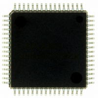
M38039FFHFP#U0 Renesas Electronics America, M38039FFHFP#U0 Datasheet - Page 62

M38039FFHFP#U0
Manufacturer Part Number
M38039FFHFP#U0
Description
IC 740 MCU FLASH 60K 64QFP
Manufacturer
Renesas Electronics America
Series
740/38000r
Datasheet
1.M38039FFHFPU0.pdf
(119 pages)
Specifications of M38039FFHFP#U0
Core Processor
740
Core Size
8-Bit
Speed
16.8MHz
Connectivity
SIO, UART/USART
Peripherals
PWM, WDT
Number Of I /o
56
Program Memory Size
60KB (60K x 8)
Program Memory Type
FLASH
Ram Size
2K x 8
Voltage - Supply (vcc/vdd)
2.7 V ~ 5.5 V
Data Converters
A/D 16x10b; D/A 2x8b
Oscillator Type
Internal
Operating Temperature
-20°C ~ 85°C
Package / Case
64-QFP
Lead Free Status / RoHS Status
Lead free / RoHS Compliant
Eeprom Size
-
Available stocks
Company
Part Number
Manufacturer
Quantity
Price
3803 Group (Spec.H)
Rev.3.11
REJ03B0017-0311
D/A CONVERTER
The 3803 group (Spec.H) has two internal D/A converters (DA
and DA
The D/A conversion is performed by setting the value in each
DA conversion register. The result of D/A conversion is output
from the DA
“1”.
When using the D/A converter, the corresponding port direction
register bit (P3
status).
The output analog voltage V is determined by the value n
(decimal notation) in the DA conversion register as follows:
V = V
At reset, the DA conversion registers are cleared to “00
the DA output enable bits are cleared to “0”, and the P3
and P3
The DA output does not have buffers. Accordingly, connect an
external buffer when driving a low-impedance load.
Fig 54. Equivalent connection circuit of D/A converter (DA1)
Where V
DA
REF
1
2
/DA
1
) with 8-bit resolution.
conversion register
P3
× n/256 (n = 0 to 255)
2
1
0
pins become high impedance.
REF
/DA
Apr 5, 2006
or DA
0
/DA
is the reference voltage.
1
AV
V
REF
2
SS
1
pin by setting the DA output enable bit to
“1”
or P3
“0”
DA
1
/DA
MSB
1
output enable bit
Page 60 of 113
“0”
2
) must be set to “0” (input
“1”
2R
R
2R
R
16
0
”, and
/DA
1
1
2R
R
Fig 53. Block diagram of D/A converter
2R
R
R-2R resistor ladder
R-2R resistor ladder
DA
DA
1
2
conversion register (8)
conversion register (8)
2R
R
2R
R
DA
DA
1
2
output enable bit
output enable bit
2R
R
LSB
2R
2R
P3
P3
0
1
/DA
/DA
2
1


