M38039FFHFP#U0 Renesas Electronics America, M38039FFHFP#U0 Datasheet - Page 116
M38039FFHFP#U0
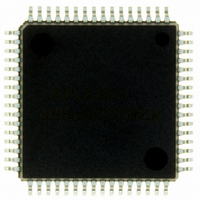
Manufacturer Part Number
M38039FFHFP#U0
Description
IC 740 MCU FLASH 60K 64QFP
Manufacturer
Renesas Electronics America
Series
740/38000r
Datasheet
1.M38039FFHFPU0.pdf
(119 pages)
Specifications of M38039FFHFP#U0
Core Processor
740
Core Size
8-Bit
Speed
16.8MHz
Connectivity
SIO, UART/USART
Peripherals
PWM, WDT
Number Of I /o
56
Program Memory Size
60KB (60K x 8)
Program Memory Type
FLASH
Ram Size
2K x 8
Voltage - Supply (vcc/vdd)
2.7 V ~ 5.5 V
Data Converters
A/D 16x10b; D/A 2x8b
Oscillator Type
Internal
Operating Temperature
-20°C ~ 85°C
Package / Case
64-QFP
Lead Free Status / RoHS Status
Lead free / RoHS Compliant
Eeprom Size
-
Available stocks
Company
Part Number
Manufacturer
Quantity
Price


Rev.
1.00
2.00
3.00
3.01
REVISION HISTORY
REVISION HISTORY
May. 28, 2003
Oct. 14, 2003
Jun.25, 2004
Sep. 3, 2001
Date
6
15
16
1,2,6,7
5
7
23
64
68
69
73
75
75,77
76,78
79
Page
–
low-speed mode
First edition issued
•Delete the following :“*:KP package is under development.”
•Table 4 pin description
V
•Fig.5 Memory expansion plan
As of Dec. 2002 → As of Mar. 2003
•Notes
(address 3A
(address 2A
•Fig.61 System clock generating circuit block diagram
•Table 10 Recommended operating conditions
Add : V
•Table 11 Recommended operating conditions
f(X
•Table 16 A/D converter characteristics
V
•Table 17 D/A converter characteristics
•Table 16 A/D converter characteristics, Table 17 D/A converter characteristics
Resolution Unit Bits → bit
•Table 18 Timing requirements (1) (In high-speed mode)
t
Min. 2.6✕10
•Table 18 Timing requirements (1) (In high-speed mode),
Table 20 Timing requirements (3) (In middle-speed mode)
t
t
•Table 19 Timing requirements (2) (In high-speed mode),
Table 20 Timing requirements (4) (In middle-speed mode)
t
•Fig.63 Timing diagram (in single-chip mode)
Delete the following underline parts :
S
T
Table 5 Pin description is partly revised.
Figure 11 Memory map of special function register (SFR) is partly revised.
Table 8 I/O port function is partly revised.
Flash memory version is added.
V
C
WH
WL
CL
High-speed or
X
CC
CC
CLK1
(X
CC
D
IN
(S
(X
(X
,V
IN
1
) High-speed mode f(φ)=f(X
8bit A/D mode, 10bit A/D mode Max. 5.0 → 5.5
= 4.0 to 5.5V → 4.0≤V
CLK2
CIN
CIN
Divider
T
) Main clock X
SS
Main clock division ratio
selection bits (Note 1)
Middle-speed mode
S
X
IL
CLK2
D
) Sub-clock input “L” pulse width → Sub-clock X
) Sub-clock input “H” pulse width → Sub-clock X
) → t
Apply voltage of 2.7–5.5V → 1.8V–5.5V
3
“L” input voltage X
S
16
16
Q
3
OUT2
/(82V
S
) → (address 003A
) → (address 002A
S
R
WL
CLK3
Prescaler 12
(S
STP instruction
FF
CC
16
Timing φ (internal clock)
CLK2
t
t
d
v
t
IN
f
(S
-3) → 26✕10
(S
(Note 3)
, t
input cycle time 2.7≤V
CLK1
CLK1
3803 Group (Spec.H) Data Sheet
(1/3)
)
r
Timer 1
01
16
-T
-T
CC
IN
Description
Reset or
STP instruction
(Note 2)
X
X
, X
≤5.5V, V
D
D
IN
1
CIN
1
16
16
)/2 2.2≤V
), t
), t
3
), (address 23
), (address 39
Summary
/(82V
v
d
1.8≤V
(S
(S
CLK2
CC
CLK2
CC
low-speed mode
High-speed or
= 2.7 to 4.0V → 2.7≤V
-3)
CC
CC
-S
-S
≤5.5V Min. → 0
≤4.0V → 2.7≤V
CC
Main clock division ratio
selection bits (Note 1)
OUT2
OUT2
Divider
Middle-speed mode
<4.0
16
16
) → (address 0039
) → (address 0023
), t
), t
Q
v
d
CIN
(S
CIN
(S
S
R
Prescaler 12
CLK3
CLK3
input “L” pulse width
STP instruction
input “H” pulse width
Timing φ (internal clock)
CC
-T
-T
(Note 3)
X
X
≤4.0V
D
D
CC
3
Timer 1
3
)
)
<4.0V
16
16
Reset or
STP instruction
(Note 2)
)
),
Reset
Related parts for M38039FFHFP#U0
Image
Part Number
Description
Manufacturer
Datasheet
Request
R

Part Number:
Description:
KIT STARTER FOR M16C/29
Manufacturer:
Renesas Electronics America
Datasheet:

Part Number:
Description:
KIT STARTER FOR R8C/2D
Manufacturer:
Renesas Electronics America
Datasheet:

Part Number:
Description:
R0K33062P STARTER KIT
Manufacturer:
Renesas Electronics America
Datasheet:

Part Number:
Description:
KIT STARTER FOR R8C/23 E8A
Manufacturer:
Renesas Electronics America
Datasheet:

Part Number:
Description:
KIT STARTER FOR R8C/25
Manufacturer:
Renesas Electronics America
Datasheet:

Part Number:
Description:
KIT STARTER H8S2456 SHARPE DSPLY
Manufacturer:
Renesas Electronics America
Datasheet:

Part Number:
Description:
KIT STARTER FOR R8C38C
Manufacturer:
Renesas Electronics America
Datasheet:

Part Number:
Description:
KIT STARTER FOR R8C35C
Manufacturer:
Renesas Electronics America
Datasheet:

Part Number:
Description:
KIT STARTER FOR R8CL3AC+LCD APPS
Manufacturer:
Renesas Electronics America
Datasheet:
Part Number:
Description:
KIT STARTER FOR RX610
Manufacturer:
Renesas Electronics America
Datasheet:

Part Number:
Description:
KIT STARTER FOR R32C/118
Manufacturer:
Renesas Electronics America
Datasheet:

Part Number:
Description:
KIT DEV RSK-R8C/26-29
Manufacturer:
Renesas Electronics America
Datasheet:

Part Number:
Description:
KIT STARTER FOR SH7124
Manufacturer:
Renesas Electronics America
Datasheet:

Part Number:
Description:
KIT STARTER FOR H8SX/1622
Manufacturer:
Renesas Electronics America
Datasheet:

Part Number:
Description:
KIT DEV FOR SH7203
Manufacturer:
Renesas Electronics America
Datasheet: