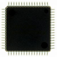
M38039FFHFP#U0 Renesas Electronics America, M38039FFHFP#U0 Datasheet - Page 64

M38039FFHFP#U0
Manufacturer Part Number
M38039FFHFP#U0
Description
IC 740 MCU FLASH 60K 64QFP
Manufacturer
Renesas Electronics America
Series
740/38000r
Datasheet
1.M38039FFHFPU0.pdf
(119 pages)
Specifications of M38039FFHFP#U0
Core Processor
740
Core Size
8-Bit
Speed
16.8MHz
Connectivity
SIO, UART/USART
Peripherals
PWM, WDT
Number Of I /o
56
Program Memory Size
60KB (60K x 8)
Program Memory Type
FLASH
Ram Size
2K x 8
Voltage - Supply (vcc/vdd)
2.7 V ~ 5.5 V
Data Converters
A/D 16x10b; D/A 2x8b
Oscillator Type
Internal
Operating Temperature
-20°C ~ 85°C
Package / Case
64-QFP
Lead Free Status / RoHS Status
Lead free / RoHS Compliant
Eeprom Size
-
Available stocks
Company
Part Number
Manufacturer
Quantity
Price
3803 Group (Spec.H)
Rev.3.11
REJ03B0017-0311
RESET CIRCUIT
To reset the microcomputer, RESET pin should be held at an “L”
level for 16 cycles or more of X
returned to an “H” level (the power source voltage should be
between 1.8 V and 5.5 V (between 2.7 V to 5.5 V for flash
memory version), and the oscillation should be stable), reset is
released. After the reset is completed, the program starts from the
address contained in address FFFD
address FFFC
voltage for the mask ROM version is less than 0.29 V for V
1.8 V.
In the flash memory version, input to the RESET pin in the
following procedure.
• When power source is stabilized
(1) Input “L” level to RESET pin.
(2) Input “L” level for 16 cycles or more to X
(3) Input “H” level to RESET pin.
• At power-on
(1) Input “L” level to RESET pin.
(2) Increase the power source voltage to 2.7 V.
(3) Wait for td(P-R) until internal power source has stabilized.
(4) Input “L” level for 16 cycles or more to X
(5) Input “H” level to RESET pin.
Fig 58. Reset sequence
Address
RESET
Internal
SYNC
reset
Data
X
IN
φ
16
Apr 5, 2006
(low-order byte). Make sure that the reset input
X
IN
: 10.5 to 18.5 clock cycles
Page 62 of 113
IN
. Then the RESET pin is
16
?
Notes 1: The frequency relation of f(X
(high-order byte) and
?
2: The question marks (?) indicate an undefined state that depends on the previous state.
IN
IN
?
pin.
pin.
?
?
CC
of
?
Fig 57. Reset circuit example
?
IN
Notes 1: Reset release voltage
RESET
RESET
) and f(φ) is f(X
?
2: In the flash memory version, this time is required td(P-R)+X
FFFC
or more.
•
•
mask ROM version: Vcc = 1.8 V
Flash memory version: Vcc = 2.7 V
IN
AD
Example at V
) = 8 • f(φ).
V
V
CC
CC
L
FFFD
Power source
voltage detection
circuit
AD
CC
= 5 V
H
AD
H
RESET
RESET
,
V
L
CC
V
0 V
0 V
5V
0V
5V
0V
CC
Reset address from the
vector table.
td(P-R)+X
2.7V
(1)
IN
16 cycles or more
(2)
0.2V
IN
CC
16 cycles
or less


