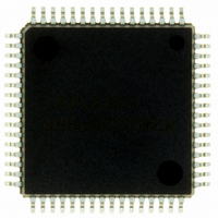
M38039FFHFP#U0 Renesas Electronics America, M38039FFHFP#U0 Datasheet - Page 50

M38039FFHFP#U0
Manufacturer Part Number
M38039FFHFP#U0
Description
IC 740 MCU FLASH 60K 64QFP
Manufacturer
Renesas Electronics America
Series
740/38000r
Datasheet
1.M38039FFHFPU0.pdf
(119 pages)
Specifications of M38039FFHFP#U0
Core Processor
740
Core Size
8-Bit
Speed
16.8MHz
Connectivity
SIO, UART/USART
Peripherals
PWM, WDT
Number Of I /o
56
Program Memory Size
60KB (60K x 8)
Program Memory Type
FLASH
Ram Size
2K x 8
Voltage - Supply (vcc/vdd)
2.7 V ~ 5.5 V
Data Converters
A/D 16x10b; D/A 2x8b
Oscillator Type
Internal
Operating Temperature
-20°C ~ 85°C
Package / Case
64-QFP
Lead Free Status / RoHS Status
Lead free / RoHS Compliant
Eeprom Size
-
Available stocks
Company
Part Number
Manufacturer
Quantity
Price
3803 Group (Spec.H)
Rev.3.11
REJ03B0017-0311
• Serial I/O2
The serial I/O2 function can be used only for clock synchronous
serial I/O.
For clock synchronous serial I/O2, the transmitter and the
receiver must use the same clock. If the internal clock is used,
transfer is started by a write signal to the serial I/O2 register
(address 001F
[Serial I/O2 Control Register (SIO2CON)] 001D
The serial I/O2 control register contains eight bits which control
various serial I/O2 functions.
Fig 39. Block diagram of serial I/O2
P5
P5
P5
P5
(f(X
3
1
2
/S
/S
/S
0
f(X
CIN
/S
OUT2
RDY2
CLK2
IN2
IN
) in low-speed mode)
)
16
Apr 5, 2006
).
S
Serial I/O2 port selection bit
Serial I/O2 port selection bit
RDY2
output enable bit
P5
“0”
“1”
“1”
“0”
“0”
P5
P5
“1”
3
1
2
latch
Page 48 of 113
latch
latch
S
RDY2
Synchronization
circuit
Serial I/O2 synchronous
clock selection bit
16
External clock
Fig 38. Structure of Serial I/O2 control register
“1”
Serial I/O counter 2 (3)
b7
“0”
Serial I/O2 register (8)
1/8
1/16
1/32
1/64
1/128
1/256
b0
Serial I/O2 control register
(SIO2CON : address 001D
Internal synchronous clock selection bits
Serial I/O2 port selection bit
S
Transfer direction selection bit
Serial I/O2 synchronous clock selection bit
P5
Address 001F
b2 b1 b0
0 0 0: f(X
0 0 1: f(X
0 1 0: f(X
0 1 1: f(X
1 1 0: f(X
1 1 1: f(X
0: I/O port
1: S
0: I/O port
1: S
0: LSB first
1: MSB first
0: External clock
1: Internal clock
0: CMOS output (in output mode)
1: N-channel open drain output (in output mode)
RDY2
1
/S
OUT2
RDY2
OUT2
output enable bit
Internal synchronous
clock selection bits
, S
signal output
P-channel output disable bit
CLK2
IN
IN
IN
IN
IN
IN
16
)/8 (f(X
)/16 (f(X
)/32 (f(X
)/64 (f(X
)/128 f(X
)/256 (f(X
signal output
Data bus
CIN
CIN
CIN
CIN
CIN
16
CIN
)/8 in low-speed mode)
)
)/16 in low-speed mode)
)/32 in low-speed mode)
)/64 in low-speed mode)
)/128 in low-speed mode)
)/256 in low-speed mode)
Serial I/O2
interrupt request


