M38039FFHFP#U0 Renesas Electronics America, M38039FFHFP#U0 Datasheet - Page 60
M38039FFHFP#U0
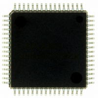
Manufacturer Part Number
M38039FFHFP#U0
Description
IC 740 MCU FLASH 60K 64QFP
Manufacturer
Renesas Electronics America
Series
740/38000r
Datasheet
1.M38039FFHFPU0.pdf
(119 pages)
Specifications of M38039FFHFP#U0
Core Processor
740
Core Size
8-Bit
Speed
16.8MHz
Connectivity
SIO, UART/USART
Peripherals
PWM, WDT
Number Of I /o
56
Program Memory Size
60KB (60K x 8)
Program Memory Type
FLASH
Ram Size
2K x 8
Voltage - Supply (vcc/vdd)
2.7 V ~ 5.5 V
Data Converters
A/D 16x10b; D/A 2x8b
Oscillator Type
Internal
Operating Temperature
-20°C ~ 85°C
Package / Case
64-QFP
Lead Free Status / RoHS Status
Lead free / RoHS Compliant
Eeprom Size
-
Available stocks
Company
Part Number
Manufacturer
Quantity
Price


3803 Group (Spec.H)
Rev.3.11
REJ03B0017-0311
A/D CONVERTER (successive approximation type)
[AD Conversion Register 1, 2 (AD1, AD2)] 0035
0038
The AD conversion register is a read-only register that stores the
result of an A/D conversion. When reading this register during an
A/D conversion, the previous conversion result is read.
Bit 7 of the AD conversion register 2 is the conversion mode
selection bit. When this bit is set to “0”, the A/D converter
becomes the 10-bit A/D mode. When this bit is set to “1”, that
becomes the 8-bit A/D mode. The conversion result of the 8-bit
A/D mode is stored in the AD conversion register 1. As for 10-bit
A/D mode, not only 10-bit reading but also only high-order 8-bit
reading of conversion result can be performed by selecting the
reading procedure of the AD conversion registers 1, 2 after A/D
conversion is completed (in Figure.51).
As for 10-bit A/D mode, the 8-bit reading inclined to MSB is
performed when reading the AD converter register 1 after A/D
conversion is started; and when the AD converter register 1 is
read after reading the AD converter register 2, the 8-bit reading
inclined to LSB is performed.
[AD/DA Control Register (ADCON)] 0034
The AD/DA control register controls the A/D conversion
process. Bits 0 to 2 and bit 4 select a specific analog input pin.
Bit 3 signals the completion of an A/D conversion. The value of
this bit remains at “0” during an A/D conversion, and changes to
“1” when an A/D conversion ends. Writing “0” to this bit starts
the A/D conversion.
• Comparison Voltage Generator
The comparison voltage generator divides the voltage between
AV
voltage in the 10-bit A/D mode (256 division in 8-bit A/D mode).
The A/D converter successively compares the comparison
voltage Vref in each mode, dividing the V
below), with the input voltage.
• 10-bit A/D mode (10-bit reading)
• 10-bit A/D mode (8-bit reading)
• 8-bit A/D mode
Vref =
Vref =
Vref =
SS
16
and V
=0
V
-------------
V
-------------
V
-------------
1024
256
256
REF
REF
REF
REF
Apr 5, 2006
× n (n = 0 − 255)
× n (n = 0 − 1023)
× (n − 0.5) (n = 1 − 255)
into 1024, and that outputs the comparison
(n = 0)
Page 58 of 113
REF
16
voltage (see
16
,
• Channel Selector
The channel selector selects one of ports P6
P0
• Comparator and Control Circuit
The comparator and control circuit compares an analog input
voltage with the comparison voltage, and then stores the result in
the AD conversion registers 1, 2. When an A/D conversion is
completed, the control circuit sets the AD conversion completion
bit and the AD interrupt request bit to “1”.
Note that because the comparator consists of a capacitor
coupling, set f(X
conversion.
Fig 50. Structure of AD/DA control register
Fig 51. Structure of 10-bit A/D mode reading
b7
7
10-bit reading
(Read address 0038
AD conversion register 2
(AD2: address 0038
AD conversion register 1
(AD1: address 0035
Note : Bits 2 to 6 of address 0038
8-bit reading
(Read only address 0035
AD conversion register 1
(AD1: address 0035
/AN
15
to P0
0
/AN
IN )
8
, and inputs the voltage to the comparator.
to 500 kHz or more during an A/D
16
16
16
16
b0
)
)
)
before 0035
16
AD/DA control register
(ADCON : address 0034
16
Analog input pin selection bits 1
AD conversion completion bit
Analog input pin selection bit 2
Not used (returns “0” when read)
DA
DA
b2 b1 b0
0 0 0: P6
0 0 1: P6
0 1 0: P6
0 1 1: P6
1 0 0: P6
1 0 1: P6
1 1 0: P6
1 1 1: P6
0: Conversion in progress
1: Conversion completed
0: AN
1: AN
0: DA
1: DA
0: DA
1: DA
become “0” at reading.
)
1
2
b7
b7
b9
b7
b7
0
output enable bit
output enable bit
0
8
1
1
2
2
b6 b5 b4 b3 b2 b1 b0
b8 b7 b6 b5 b4 b3 b2
to AN
to AN
output disabled
output enabled
output disabled
output enabled
0
1
2
3
4
5
6
7
16
7
/AN
/AN
/AN
/AN
/AN
/AN
/AN
/AN
/AN
7
15
)
side
0 or
1 or
2 or
3 or
4 or
5 or
6 or
7 or
side
7
to P6
P0
P0
P0
P0
P0
P0
P0
P0
16
0
1
2
3
4
5
6
7
b9 b8
0
/AN
/AN
/AN
/AN
/AN
/AN
/AN
/AN
/AN
)
b0
b0
b0
8
9
10
11
12
13
14
15
0
or
Related parts for M38039FFHFP#U0
Image
Part Number
Description
Manufacturer
Datasheet
Request
R

Part Number:
Description:
KIT STARTER FOR M16C/29
Manufacturer:
Renesas Electronics America
Datasheet:

Part Number:
Description:
KIT STARTER FOR R8C/2D
Manufacturer:
Renesas Electronics America
Datasheet:

Part Number:
Description:
R0K33062P STARTER KIT
Manufacturer:
Renesas Electronics America
Datasheet:

Part Number:
Description:
KIT STARTER FOR R8C/23 E8A
Manufacturer:
Renesas Electronics America
Datasheet:

Part Number:
Description:
KIT STARTER FOR R8C/25
Manufacturer:
Renesas Electronics America
Datasheet:

Part Number:
Description:
KIT STARTER H8S2456 SHARPE DSPLY
Manufacturer:
Renesas Electronics America
Datasheet:

Part Number:
Description:
KIT STARTER FOR R8C38C
Manufacturer:
Renesas Electronics America
Datasheet:

Part Number:
Description:
KIT STARTER FOR R8C35C
Manufacturer:
Renesas Electronics America
Datasheet:

Part Number:
Description:
KIT STARTER FOR R8CL3AC+LCD APPS
Manufacturer:
Renesas Electronics America
Datasheet:
Part Number:
Description:
KIT STARTER FOR RX610
Manufacturer:
Renesas Electronics America
Datasheet:

Part Number:
Description:
KIT STARTER FOR R32C/118
Manufacturer:
Renesas Electronics America
Datasheet:

Part Number:
Description:
KIT DEV RSK-R8C/26-29
Manufacturer:
Renesas Electronics America
Datasheet:

Part Number:
Description:
KIT STARTER FOR SH7124
Manufacturer:
Renesas Electronics America
Datasheet:

Part Number:
Description:
KIT STARTER FOR H8SX/1622
Manufacturer:
Renesas Electronics America
Datasheet:

Part Number:
Description:
KIT DEV FOR SH7203
Manufacturer:
Renesas Electronics America
Datasheet: