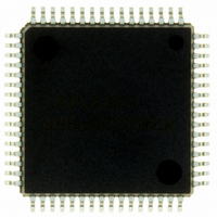
M38039FFHFP#U0 Renesas Electronics America, M38039FFHFP#U0 Datasheet - Page 73

M38039FFHFP#U0
Manufacturer Part Number
M38039FFHFP#U0
Description
IC 740 MCU FLASH 60K 64QFP
Manufacturer
Renesas Electronics America
Series
740/38000r
Datasheet
1.M38039FFHFPU0.pdf
(119 pages)
Specifications of M38039FFHFP#U0
Core Processor
740
Core Size
8-Bit
Speed
16.8MHz
Connectivity
SIO, UART/USART
Peripherals
PWM, WDT
Number Of I /o
56
Program Memory Size
60KB (60K x 8)
Program Memory Type
FLASH
Ram Size
2K x 8
Voltage - Supply (vcc/vdd)
2.7 V ~ 5.5 V
Data Converters
A/D 16x10b; D/A 2x8b
Oscillator Type
Internal
Operating Temperature
-20°C ~ 85°C
Package / Case
64-QFP
Lead Free Status / RoHS Status
Lead free / RoHS Compliant
Eeprom Size
-
Available stocks
Company
Part Number
Manufacturer
Quantity
Price
3803 Group (Spec.H)
Rev.3.11
REJ03B0017-0311
Fig 67. Structure of flash memory control register 2
Table 12 State of E/W inhibition function
Figure.68 shows a flowchart for setting/releasing CPU rewrite mode.
Fig 68. CPU rewrite mode set/release flowchart be sure to execute
All user block E/W
Notes 1: For this bit to be set to “1”, the user needs to write a “0” and then a
b7
enable bit
2: Effective only when the CPU rewrite mode select bit = “1”.
0
0
1
1
“1” to it in succession. For this bit to be set to “0”, write “0” only to this
bit.
Apr 5, 2006
Notes 1: Set the main clock as follows depending on the clock division ratio selection bits of CPU mode register (bits 6, 7 of address 003B
8 KB user block
E/W enable bit
b0
2: Before exiting the CPU rewrite mode after completing erase or program operation, always be sure to execute the read array
Flash memory control register 2
(FMCR2: address : 0FE2
Not used
Not used (do not write “1” to this bit.)
Not used
All user block E/W enable bit
0 : E/W disabled
1 : E/W enabled
Not used
command.
0
1
0
1
Page 71 of 113
Addresses C000
16
: initial value: 45
8 KB × 2 block
E/W disabled
E/W disabled
E/W disabled
E/W enabled
(1, 2)
Single-chip mode or Boot mode
Set CPU mode register
Jump to control program transferred to internal RAM
(Subsequent operations are executed by control program in
this RAM)
Set CPU rewrite mode select bit to “1” (by writing “0” and
then “1” in succession)
Set all user block E/W enable bit to “1” (by writing “0” and
then “1” in succession)
Set 8 KB user block E/W enable bit (At E/W disabled; writing
“0” , at E/W enabled;
writing “0” and then “1” in succession
Using software command executes erase, program, or other
operation
Execute read array command
Set all user block E/W enable bit to “0”
Set 8 KB user block E/W enable bit to “0”
Transfer CPU rewrite mode control program to internal RAM
Write “0” to CPU rewrite mode select bit
16
to FFFF
16
)
(1)
Start
End
16
(2)
Addresses 2000
16 KB + 24 KB block
E/W disabled
E/W disabled
E/W enabled
E/W enabled
16
to BFFF
16
Addresses 1000
16
).
E/W enabled
E/W enabled
E/W enabled
E/W enabled
Data block
16
to 1FFF
16


