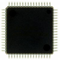
M38039FFHFP#U0 Renesas Electronics America, M38039FFHFP#U0 Datasheet - Page 83

M38039FFHFP#U0
Manufacturer Part Number
M38039FFHFP#U0
Description
IC 740 MCU FLASH 60K 64QFP
Manufacturer
Renesas Electronics America
Series
740/38000r
Datasheet
1.M38039FFHFPU0.pdf
(119 pages)
Specifications of M38039FFHFP#U0
Core Processor
740
Core Size
8-Bit
Speed
16.8MHz
Connectivity
SIO, UART/USART
Peripherals
PWM, WDT
Number Of I /o
56
Program Memory Size
60KB (60K x 8)
Program Memory Type
FLASH
Ram Size
2K x 8
Voltage - Supply (vcc/vdd)
2.7 V ~ 5.5 V
Data Converters
A/D 16x10b; D/A 2x8b
Oscillator Type
Internal
Operating Temperature
-20°C ~ 85°C
Package / Case
64-QFP
Lead Free Status / RoHS Status
Lead free / RoHS Compliant
Eeprom Size
-
Available stocks
Company
Part Number
Manufacturer
Quantity
Price
3803 Group (Spec.H)
Rev.3.11
REJ03B0017-0311
Table 15 Description of pin function (Flash Memory Serial I/O Mode 1)
Table 16 Description of pin function (Flash Memory Serial I/O Mode 2)
V
CNV
RESET
X
X
AV
V
P0
P2
P4
P6
P4
P4
P4
P4
V
CNV
RESET
X
X
AV
V
P0
P2
P4
P6
P4
P4
P4
P4
CC
IN
OUT
REF
CC
IN
OUT
REF
SS
0
0
0
0
4
5
6
7
SS
0
0
0
0
4
5
6
7
−P0
−P2
−P4
−P6
−P0
−P2
−P4
−P6
,V
,V
SS
SS
SS
SS
Pin name
Pin name
7
7
3
7
7
7
3
7
, P1
, P3
, P5
, P1
, P3
, P5
0
0
0
0
0
0
Apr 5, 2006
−P1
−P3
−P5
−P1
−P3
−P5
7
7
7
7
7
7
,
,
,
,
,
,
Power supply
CNV
Reset input
Clock input
Clock output
Analog power supply input
Reference voltage input
I/O port
RxD input
TxD output
S
BUSY output
Power supply
CNV
Reset input
Clock input
Clock output
Analog power supply input
Reference voltage input
I/O port
RxD input
TxD output
S
BUSY output
CLK
CLK
SS
SS
input
input
Signal name
Signal name
Page 81 of 113
I/O
I/O
I/O
I/O
O
O
O
O
O
O
I
I
I
I
I
I
I
I
I
I
I
I
I
I
Apply 2.7 to 5.5 V to the V
After input of port is set, input “H” level.
Reset input pin. To reset the microcomputer, RESET pin should be
held at an “L” level for 16 cycles or more of X
Connect an oscillation circuit between the X
As for the connection method, refer to the “clock generating circuit”.
Connect AVss to V
Apply reference voltage of A/D to this pin.
Input “L” or “H” level, or keep open.
Serial data input pin.
Serial data output pin.
Serial clock input pin.
BUSY signal output pin.
Apply 2.7 to 5.5 V to the Vcc pin and 0 V to the V
After input of port is set, input “H” level.
Reset input pin. To reset the microcomputer, RESET pin should be
held at an “L” level for 16 cycles or more of X
Connect an oscillation circuit between the X
As for the connection method, refer to the “clock generating circuit”.
Connect AVss to V
Apply reference voltage of A/D to this pin.
Input “L” or “H” level, or keep open.
Serial data input pin.
Serial data output pin.
Input “L” level.
BUSY signal output pin.
SS
SS
.
.
CC
Function
pin and 0 V to the Vss pin.
Function
IN
IN
IN
IN
and X
and X
.
.
SS
OUT
pin.
OUT
pins.
pins.


