M38039FFHFP#U0 Renesas Electronics America, M38039FFHFP#U0 Datasheet - Page 95
M38039FFHFP#U0
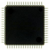
Manufacturer Part Number
M38039FFHFP#U0
Description
IC 740 MCU FLASH 60K 64QFP
Manufacturer
Renesas Electronics America
Series
740/38000r
Datasheet
1.M38039FFHFPU0.pdf
(119 pages)
Specifications of M38039FFHFP#U0
Core Processor
740
Core Size
8-Bit
Speed
16.8MHz
Connectivity
SIO, UART/USART
Peripherals
PWM, WDT
Number Of I /o
56
Program Memory Size
60KB (60K x 8)
Program Memory Type
FLASH
Ram Size
2K x 8
Voltage - Supply (vcc/vdd)
2.7 V ~ 5.5 V
Data Converters
A/D 16x10b; D/A 2x8b
Oscillator Type
Internal
Operating Temperature
-20°C ~ 85°C
Package / Case
64-QFP
Lead Free Status / RoHS Status
Lead free / RoHS Compliant
Eeprom Size
-
Available stocks
Company
Part Number
Manufacturer
Quantity
Price


3803 Group (Spec.H)
Rev.3.11
REJ03B0017-0311
Electrical characteristics
Table 21 Electrical characteristics (1)
NOTE:
V
V
V
V
V
V
I
I
I
I
I
I
I
V
IH
IH
IH
IL
IL
IL
IL
OH
OL
OL
T+
T+
T+
RAM
1. P3
Symbol
− V
− V
− V
P4
T
T
T
5
5
−
−
−
is measured when the P3
is measured when the P4
(Mask ROM version: V
(Flash memory version: V
Apr 5, 2006
“H” output voltage
“L” output voltage
“L” output voltage
Hysteresis
Hysteresis
Hysteresis
“H” input current
“H” input current
“H” input current
“L” input current
“L” input current
“L” input current
“L” input current (at Pull-up)
RAM hold voltage
P0
P3
P0
P4
P2
CNTR
RxD
RESET
P0
P4
RESET, CNV
X
P0
P4
RESET, CNV
X
P0
P3
IN
IN
0
4
0
0
0
0
0
0
0
0
4
-P0
-P3
-P0
-P4
-P2
-P0
-P4
-P0
-P4
-P0
-P3
1
, S
0
7
7
7
7
7
, CNTR
7
7
7
7
7
7
, P1
, P4
, P1
, P5
CLK1
, P1
, P5
, P1
, P5
, P1
, P4
0
0
0
0
0
0
0
0
0
0
, S
-P1
-P4
-P1
-P5
-P1
-P5
-P1
-P5
-P1
-P4
SS
SS
1
IN2
Parameter
, CNTR
(1)
7
7
7
7
7
7
7
7
7
7
Page 93 of 113
, P2
, P5
, P2
, P6
, P2
, P6
, P2
, P6
, P2
, P5
, S
5
5
/T
/T
CC
CLK2
X
X
0
0
0
0
0
0
0
0
0
0
-P2
-P5
-P2
-P6
-P2
-P6
-P2
-P6
-P2
-P5
D
D
2
CC
= 1.8 to 5.5 V, V
, INT
3
1
, RxD
P-channel output disable bit of the UART3 control register (bit 4 of address 0033
P-channel output disable bit of the UART1 control register (bit 4 of address 001B
7
7
7
7
7
7
7
7
7
7
, P3
, P6
, P3
, P3
, P3
, P3
, P6
= 2.7 to 5.5 V, V
0
-INT
3
0
0
0
0
0
0
0
, S
, P3
-P6
-P3
-P3
-P3
, P3
-P6
CLK3
4
7
7
7
7
7
1
1
,
,
,
,
,
SS
I
V
I
V
I
V
I
V
I
V
I
V
V
(Pin floating,
Pull-up transistor “off”)
V
V
V
(Pin floating,
Pull-up transistor “off”)
V
V
V
V
V
V
When clock stopped
OH
OH
OL
OL
OL
OL
= 0V, Ta = –20 to 85 °C, unless otherwise noted)
SS
CC
CC
CC
CC
CC
CC
I
I
I
I
I
I
I
CC
I
CC
= V
= V
= V
= V
= V
= V
= V
= V
= 10 mA
= 1.6 mA
= 20 mA
= 1.6 mA
= −10 mA
= –1.0 mA
= 0V, Ta = –20 to 85 °C, unless otherwise noted)
= 5.0 V
= 3.0 V
= 4.0 to 5.5 V
= 1.8 to 5.5 V
= 4.0 to 5.5 V
= 1.8 to 5.5 V
= 4.0 to 5.5 V
= 1.8 to 5.5 V
Test conditions
CC
CC
CC
SS
SS
SS
SS
SS
V
V
CC
CC
Min.
−80
−30
1.8
− 2.0
− 1.0
Limits
−210
Typ.
−4.0
−70
0.4
0.5
0.5
4.0
−420
−140
Max.
−5.0
−5.0
V
2.0
1.0
2.0
0.4
5.0
5.0
CC
16
16
) is “0”.
) is “0”.
Unit
µA
µA
µA
µA
µA
µA
µA
V
V
V
V
V
V
V
Related parts for M38039FFHFP#U0
Image
Part Number
Description
Manufacturer
Datasheet
Request
R

Part Number:
Description:
KIT STARTER FOR M16C/29
Manufacturer:
Renesas Electronics America
Datasheet:

Part Number:
Description:
KIT STARTER FOR R8C/2D
Manufacturer:
Renesas Electronics America
Datasheet:

Part Number:
Description:
R0K33062P STARTER KIT
Manufacturer:
Renesas Electronics America
Datasheet:

Part Number:
Description:
KIT STARTER FOR R8C/23 E8A
Manufacturer:
Renesas Electronics America
Datasheet:

Part Number:
Description:
KIT STARTER FOR R8C/25
Manufacturer:
Renesas Electronics America
Datasheet:

Part Number:
Description:
KIT STARTER H8S2456 SHARPE DSPLY
Manufacturer:
Renesas Electronics America
Datasheet:

Part Number:
Description:
KIT STARTER FOR R8C38C
Manufacturer:
Renesas Electronics America
Datasheet:

Part Number:
Description:
KIT STARTER FOR R8C35C
Manufacturer:
Renesas Electronics America
Datasheet:

Part Number:
Description:
KIT STARTER FOR R8CL3AC+LCD APPS
Manufacturer:
Renesas Electronics America
Datasheet:
Part Number:
Description:
KIT STARTER FOR RX610
Manufacturer:
Renesas Electronics America
Datasheet:

Part Number:
Description:
KIT STARTER FOR R32C/118
Manufacturer:
Renesas Electronics America
Datasheet:

Part Number:
Description:
KIT DEV RSK-R8C/26-29
Manufacturer:
Renesas Electronics America
Datasheet:

Part Number:
Description:
KIT STARTER FOR SH7124
Manufacturer:
Renesas Electronics America
Datasheet:

Part Number:
Description:
KIT STARTER FOR H8SX/1622
Manufacturer:
Renesas Electronics America
Datasheet:

Part Number:
Description:
KIT DEV FOR SH7203
Manufacturer:
Renesas Electronics America
Datasheet: