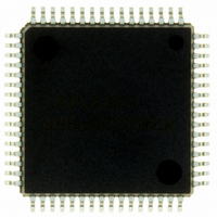
M38039FFHFP#U0 Renesas Electronics America, M38039FFHFP#U0 Datasheet - Page 75

M38039FFHFP#U0
Manufacturer Part Number
M38039FFHFP#U0
Description
IC 740 MCU FLASH 60K 64QFP
Manufacturer
Renesas Electronics America
Series
740/38000r
Datasheet
1.M38039FFHFPU0.pdf
(119 pages)
Specifications of M38039FFHFP#U0
Core Processor
740
Core Size
8-Bit
Speed
16.8MHz
Connectivity
SIO, UART/USART
Peripherals
PWM, WDT
Number Of I /o
56
Program Memory Size
60KB (60K x 8)
Program Memory Type
FLASH
Ram Size
2K x 8
Voltage - Supply (vcc/vdd)
2.7 V ~ 5.5 V
Data Converters
A/D 16x10b; D/A 2x8b
Oscillator Type
Internal
Operating Temperature
-20°C ~ 85°C
Package / Case
64-QFP
Lead Free Status / RoHS Status
Lead free / RoHS Compliant
Eeprom Size
-
Available stocks
Company
Part Number
Manufacturer
Quantity
Price
3803 Group (Spec.H)
Rev.3.11
REJ03B0017-0311
Software Commands
Table 13 lists the software commands.
After setting the CPU rewrite mode select bit to “1”, execute a
software command to specify an erase or program operation.
Each software command is explained below.
• Read Array Command (FF
The read array mode is entered by writing the command code
“FF
in one of the bus cycles that follow, the contents of the specified
address are read out at the data bus (D
The read array mode is retained until another command is
written.
• Read Status Register Command (70
When the command code “70
the contents of the status register are read out at the data bus (D
to D
The status register is explained in the next section.
• Clear Status Register Command (50
This command is used to clear the bits SR4 and SR5 of the status
register after they have been set. These bits indicate that
operation has ended in an error. To use this command, write the
command code “50
• Program Command (40
Program operation starts when the command code “40
written in the first bus cycle. Then, if the address and data to
program are written in the 2nd bus cycle, program operation
(data programming and verification) will start.
Whether the write operation is completed can be confirmed by
read status register or the RY/BY status flag. When the program
starts, the read status register mode is entered automatically and
the contents of the status register is read at the data bus (D
D
the write operation starts and is returned to “1” upon completion
of the write operation. In this case, the read status register mode
remains active until the read array command (FF
Table 13 List of software commands (CPU rewrite mode)
NOTES:
7
Read array
Read status register
Clear status register
Program
Block erase
1. SRD = Status Register Data
2. WA = Write Address, WD = Write Data
3. BA = Block Address to be erased (Input the maximum address of each block.)
4. X denotes a given address in the User ROM area.
). The status register bit 7 (SR7) is set to “0” at the same time
16
7
) by a read in the second bus cycle.
” in the first bus cycle. When an address to be read is input
Command
Apr 5, 2006
16
” in the first bus cycle.
16
number
cycle
)
16
1
2
1
2
2
16
)
” is written in the first bus cycle,
Page 73 of 113
16
16
0
)
to D
)
Mode
Write
Write
Write
Write
Write
7
).
16
) is written.
First bus cycle
Address
X
16
X
X
X
X
(4)
” is
0
to
0
The RY/BY status flag of the flash memory control register is
“0” during write operation and “1” when the write operation is
completed as is the status register bit 7.
At program end, program results can be checked by reading the
status register.
Fig 69. Program flowchart
(D
0
Data
FF
70
50
40
20
to D
16
16
16
16
16
Write
7
Read status register
)
Program completed
Write “40
Write address
Write data
RY/BY =
SR4 = “0”?
SR7 =
Start
or
Mode
Read
Write
Write
“
YES
1
YES
“
1
”
16
?
”
?
”
Second bus cycle
NO
NO
Address
WA
BA
X
(3)
(2)
Program error
(D
SRD
WD
0
Data
D0
to D
16
(2)
(1)
7
)


