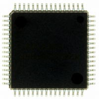
M38039FFHFP#U0 Renesas Electronics America, M38039FFHFP#U0 Datasheet - Page 109

M38039FFHFP#U0
Manufacturer Part Number
M38039FFHFP#U0
Description
IC 740 MCU FLASH 60K 64QFP
Manufacturer
Renesas Electronics America
Series
740/38000r
Datasheet
1.M38039FFHFPU0.pdf
(119 pages)
Specifications of M38039FFHFP#U0
Core Processor
740
Core Size
8-Bit
Speed
16.8MHz
Connectivity
SIO, UART/USART
Peripherals
PWM, WDT
Number Of I /o
56
Program Memory Size
60KB (60K x 8)
Program Memory Type
FLASH
Ram Size
2K x 8
Voltage - Supply (vcc/vdd)
2.7 V ~ 5.5 V
Data Converters
A/D 16x10b; D/A 2x8b
Oscillator Type
Internal
Operating Temperature
-20°C ~ 85°C
Package / Case
64-QFP
Lead Free Status / RoHS Status
Lead free / RoHS Compliant
Eeprom Size
-
Available stocks
Company
Part Number
Manufacturer
Quantity
Price
3803 Group (Spec.H)
Rev.3.11
REJ03B0017-0311
NOTES ON PERIPHERAL FUNCTIONS
Notes on Input and Output Ports
1. Notes in standby state
In standby state
levels of an I/O port “undefined”. Even when an I/O port of
Nchannel open-drain is set as output mode, if output data is “1”,
the aforementioned notes are necessary.
Pull-up (connect the port to V
to V
When determining a resistance value, note the following points:
• External circuit
• Variation of output levels during the ordinary operation
When using built-in pull-up resistor, note on varied current
values:
• When setting as an input port : Fix its input level
• When setting as an output port : Prevent current from flowing
<Reason>
Exclusive input ports are always in a high-impedance state. An
output transistor becomes an OFF state when an I/O port is set as
input mode by the direction register, so that the port enter a
highimpedance state. At this time, the potential which is input to
the input buffer in a microcomputer is unstable in the state that
input levels are “undefined”. This may cause power source
current.
Even when an I/O port of N-channel open-drain is set as output
mode by the direction register, if the contents of the port latch is
“1”, the same phenomenon as that of an input port will occur.
*1
2. Modifying output data with bit managing instruction
When the port latch of an I/O port is modified with the bit
managing instruction
changed.
<Reason>
The bit managing instructions are read-modify-write form
instructions for reading and writing data by a byte unit.
Accordingly, when these instructions are executed on a bit of the
port latch of an I/O port, the following is executed to all bits of
the port latch.
• As for bit which is set for input port:
• As for bit which is set for output port:
Note the following:
• Even when a port which is set as an output port is changed for
• As for a bit of which is set for an input port, its value may be
*2
out to external
The pin state is read in the CPU, and is written to this bit after
bit managing.
The bit value is read in the CPU, and is written to this bit after
bit managing.
an input port, its port latch holds the output data.
changed even when not specified with a bit managing
instruction in case where the pin state differs from its port latch
contents.
Standby state :
Bit managing instructions : SEB, and CLB instructions
SS
) these ports through a resistor.
Apr 5, 2006
*1
for low-power dissipation, do not make input
stop mode by executing STP instruction
wait mode by executing WIT instruction
*2
, the value of the unspecified bit may be
CC
) or pull-down (connect the port
Page 107 of 113
Termination of Unused Pins
1. Terminate unused pins
(1) Output ports : Open
(2) I/O ports :
• Set the I/O ports for the input mode and connect them to V
• When opening them in the output mode, the input mode of the
• Since the direction register setup may be changed because of a
(3) The AV
• When not using the A/D converter, handle a power source pin
2. Termination remarks
(1) I/O ports :
Do not open in the input mode.
<Reason>
• The power source current may increase depending on the
• An effect due to noise may be easily produced as compared
(2) I/O ports :
When setting for the input mode, do not connect to V
directly.
<Reason>
If the direction register setup changes for the output mode
because of a program runaway or noise, a short circuit may occur
between a port and V
(3) I/O ports :
When setting for the input mode, do not connect multiple ports in
a lump to V
<Reason>
If the direction register setup changes for the output mode
because of a program runaway or noise, a short circuit may occur
between ports.
• At the termination of unused pins, perform wiring at the
or V
Ports that permit the selecting of a built-in pull-up resistor can
also use this resistor. Set the I/O ports for the output mode and
open them at “L” or “H”.
initial status remains until the mode of the ports is switched
over to the output mode by the program after reset. Thus, the
potential at these pins is undefined and the power source
current may increase in the input mode. With regard to an
effects on the system, thoroughly perform system evaluation
on the user side.
program runaway or noise, set direction registers by program
periodically to increase the reliability of program.
for the A/D converter, AV
AV
firststage circuit.
with proper termination (2) in 1 and shown on the above.
shortest possible distance (20 mm or less) from micro-
computer pins.
SS
SS
: Connect to the V
through each resistor of 1 kΩ to 10 kΩ.
CC
SS
or V
pin when not using the A/D converter :
SS
CC
through a resistor.
(or V
SS
SS
pin.
SS
pin as follows:
).
CC
or V
CC
SS


