M38039FFHFP#U0 Renesas Electronics America, M38039FFHFP#U0 Datasheet - Page 9
M38039FFHFP#U0
Manufacturer Part Number
M38039FFHFP#U0
Description
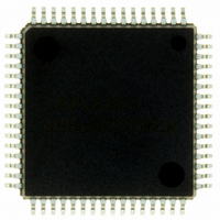
IC 740 MCU FLASH 60K 64QFP
Manufacturer
Renesas Electronics America
Series
740/38000r
Datasheet
1.M38039FFHFPU0.pdf
(119 pages)
Specifications of M38039FFHFP#U0
Core Processor
740
Core Size
8-Bit
Speed
16.8MHz
Connectivity
SIO, UART/USART
Peripherals
PWM, WDT
Number Of I /o
56
Program Memory Size
60KB (60K x 8)
Program Memory Type
FLASH
Ram Size
2K x 8
Voltage - Supply (vcc/vdd)
2.7 V ~ 5.5 V
Data Converters
A/D 16x10b; D/A 2x8b
Oscillator Type
Internal
Operating Temperature
-20°C ~ 85°C
Package / Case
64-QFP
Lead Free Status / RoHS Status
Lead free / RoHS Compliant
Eeprom Size
-
Available stocks
Company
Part Number
Manufacturer
Quantity
Price


3803 Group (Spec.H)
Rev.3.11
REJ03B0017-0311
PIN DESCRIPTION
Table 6
V
CNV
V
AV
RESET
X
X
P0
P0
P1
P1
P1
P2
P3
P3
P3
P3
P3
P3
P3
P4
P4
P4
P4
P4
P4
P4
P4
P5
P5
P5
P5
P5
P5
P5
P5
P6
P6
CC
REF
IN
OUT
1
SS
0
7
0
2
0
0
1
2
4
5
6
7
0
1
2
3
4
5
6
7
0
1
2
3
4
5
6
7
0
7
/INT
/AN
/AN
/INT
−P1
-P2
/DA
/DA
, P3
/R
/T
/S
/S
/INT
/INT
/INT
/INT
/R
/T
/S
/S
/S
/S
/S
/S
/CNTR
/CNTR
/PWM
/INT
/AN
/AN
, V
SS
X
X
CLK3
RDY3
CLK1
RDY1
IN2
OUT2
CLK2
RDY2
X
X
SS
D
D
7
D
D
Pin
8
15
1
2
0
7
7
3
01
41
40
00
1
2
3
−
3
1
−
3
1
/X
/X
/CNTR
0
1
Pin description
COUT
CIN
Apr 5, 2006
2
Power source
CNV
Reference
voltage
Analog power
source
Reset input
Main clock input • Input and output pins for the clock generating circuit.
Main clock
output
I/O port P0
I/O port P1
I/O port P2
I/O port P3
I/O port P4
I/O port P5
I/O port P6
SS
Name
input
Page 7 of 113
• Apply voltage of 1.8 V − 5.5 V to V
• This pin controls the operation mode of the chip.
• Normally connected to V
• Reference voltage input pin for A/D and D/A converters.
• Analog power source input pin for A/D and D/A converters.
• Connect to V
• Reset input pin for active “L”.
• Connect a ceramic resonator or quartz-crystal oscillator between the X
• When an external clock is used, connect the clock source to the X
• 8-bit CMOS I/O port.
• I/O direction register allows each pin to be individually
• CMOS compatible input level.
• CMOS 3-state output structure.
• Pull-up control is enabled in a bit unit.
• P2
• 8-bit CMOS I/O port.
• I/O direction register allows each pin to be individually
• CMOS compatible input level.
• P3
• P3
• Pull-up control of P3
• 8-bit CMOS I/O port.
• I/O direction register allows each pin to be individually
• CMOS compatible input level.
• CMOS 3-state output structure.
• Pull-up control is enabled in a bit unit.
voltage of 2.7 V − 5.5 V to Vcc.
the oscillation frequency.
open.
programmed as either input or output.
LED drive.
programmed as either input or output.
programmed as either input or output.
0
0
2
, P3
, P3
− P2
1
3
, P3
7
are N-channel open-drain output structure.
(8 bits) are enabled to output large current for
4
SS
− P3
.
7
0
are CMOS 3-state output structure.
, P3
Functions
SS
1
, P3
.
4
− P3
CC
7
, and 0 V to V
is enabled in a bit unit.
SS
. In the flash memory version, apply
• A/D converter input pin
• Interrupt input pin
• D/A converter input pin
• Serial I/O3 function pin
• Interrupt input pin
• Sub-clock generating I/O pin
• Interrupt input pin
• Serial I/O1 function pin
• Serial I/O1, timer Z function pin
• Serial I/O2 function pin
• Timer X function pin
• Timer Y function pin
• PWM output pin
• Interrupt input pin
• A/D converter input pin
Function except a port function
(resonator connected)
IN
pin and leave the X
IN
and X
OUT
pins to set
OUT
pin
Related parts for M38039FFHFP#U0
Image
Part Number
Description
Manufacturer
Datasheet
Request
R

Part Number:
Description:
KIT STARTER FOR M16C/29
Manufacturer:
Renesas Electronics America
Datasheet:

Part Number:
Description:
KIT STARTER FOR R8C/2D
Manufacturer:
Renesas Electronics America
Datasheet:

Part Number:
Description:
R0K33062P STARTER KIT
Manufacturer:
Renesas Electronics America
Datasheet:

Part Number:
Description:
KIT STARTER FOR R8C/23 E8A
Manufacturer:
Renesas Electronics America
Datasheet:

Part Number:
Description:
KIT STARTER FOR R8C/25
Manufacturer:
Renesas Electronics America
Datasheet:

Part Number:
Description:
KIT STARTER H8S2456 SHARPE DSPLY
Manufacturer:
Renesas Electronics America
Datasheet:

Part Number:
Description:
KIT STARTER FOR R8C38C
Manufacturer:
Renesas Electronics America
Datasheet:

Part Number:
Description:
KIT STARTER FOR R8C35C
Manufacturer:
Renesas Electronics America
Datasheet:

Part Number:
Description:
KIT STARTER FOR R8CL3AC+LCD APPS
Manufacturer:
Renesas Electronics America
Datasheet:
Part Number:
Description:
KIT STARTER FOR RX610
Manufacturer:
Renesas Electronics America
Datasheet:

Part Number:
Description:
KIT STARTER FOR R32C/118
Manufacturer:
Renesas Electronics America
Datasheet:

Part Number:
Description:
KIT DEV RSK-R8C/26-29
Manufacturer:
Renesas Electronics America
Datasheet:

Part Number:
Description:
KIT STARTER FOR SH7124
Manufacturer:
Renesas Electronics America
Datasheet:

Part Number:
Description:
KIT STARTER FOR H8SX/1622
Manufacturer:
Renesas Electronics America
Datasheet:

Part Number:
Description:
KIT DEV FOR SH7203
Manufacturer:
Renesas Electronics America
Datasheet: