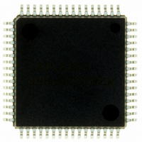
M38039FFHFP#U0 Renesas Electronics America, M38039FFHFP#U0 Datasheet - Page 49

M38039FFHFP#U0
Manufacturer Part Number
M38039FFHFP#U0
Description
IC 740 MCU FLASH 60K 64QFP
Manufacturer
Renesas Electronics America
Series
740/38000r
Datasheet
1.M38039FFHFPU0.pdf
(119 pages)
Specifications of M38039FFHFP#U0
Core Processor
740
Core Size
8-Bit
Speed
16.8MHz
Connectivity
SIO, UART/USART
Peripherals
PWM, WDT
Number Of I /o
56
Program Memory Size
60KB (60K x 8)
Program Memory Type
FLASH
Ram Size
2K x 8
Voltage - Supply (vcc/vdd)
2.7 V ~ 5.5 V
Data Converters
A/D 16x10b; D/A 2x8b
Oscillator Type
Internal
Operating Temperature
-20°C ~ 85°C
Package / Case
64-QFP
Lead Free Status / RoHS Status
Lead free / RoHS Compliant
Eeprom Size
-
Available stocks
Company
Part Number
Manufacturer
Quantity
Price
3803 Group (Spec.H)
Rev.3.11
REJ03B0017-0311
3. S
• Note
4. Setting serial I/O1 control register again
• Note
5.Data transmission control with referring to transmit shift
• Note
6. Transmission control when external clock is selected
• Note
When signals are output from the S
side by using an external clock in the clock synchronous serial
I/O mode, set all of the receive enable bit, the S
enable bit, and the transmit enable bit to “1” (transmit
enabled).
Set the serial I/O1 control register again after the transmission
and the reception circuits are reset by clearing both the
transmit enable bit and the receive enable bit to “0”.
After the transmit data is written to the transmit buffer register,
the transmit shift register completion flag changes from “1” to
“0” with a delay of 0.5 to 1.5 shift clocks. When data
transmission is controlled with referring to the flag after
writing the data to the transmit buffer register, note the delay.
When an external clock is used as the synchronous clock for
data transmission, set the transmit enable bit to “1” at “H” of
the S
register at “H” of the S
register completion flag
Clear both the transmit enable
bit (TE) and the receive enable
bit (RE) to “0”
Set the bits 0 to 3 and bit 6 of
the serial I/O1 control register
Set both the transmit enable bit
(TE) and the receive enable bit
(RE), or one of them to “1”
RDY1
CLK1
output of reception side
input level. Also, write data to the transmit buffer
Apr 5, 2006
CLK1
input level.
Page 47 of 113
RDY1
Can be set with the
LDM instruction at
the same time
pin on the reception
RDY1
output
7. Transmit interrupt request when transmit enable bit is set
• Note
• Reason
When using the transmit interrupt, take the following
sequence.
When the transmit enable bit is set to “1”, the transmit buffer
empty flag and the transmit shift register shift completion flag
are also set to “1”. Therefore, regardless of selecting which
timing for the generating of transmit interrupts, the interrupt
request is generated and the transmit interrupt request bit is set
at this point.
1. Set the serial I/O1 transmit interrupt enable bit to “0” (dis-
2. Set the transmit enable bit to “1”.
3. Set the serial I/O1 transmit interrupt request bit to “0” after
4. Set the serial I/O1 transmit interrupt enable bit to “1”
abled).
1 or more instruction has executed.
(enabled).


