M38039FFHFP#U0 Renesas Electronics America, M38039FFHFP#U0 Datasheet - Page 117
M38039FFHFP#U0
Manufacturer Part Number
M38039FFHFP#U0
Description
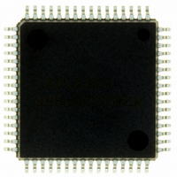
IC 740 MCU FLASH 60K 64QFP
Manufacturer
Renesas Electronics America
Series
740/38000r
Datasheet
1.M38039FFHFPU0.pdf
(119 pages)
Specifications of M38039FFHFP#U0
Core Processor
740
Core Size
8-Bit
Speed
16.8MHz
Connectivity
SIO, UART/USART
Peripherals
PWM, WDT
Number Of I /o
56
Program Memory Size
60KB (60K x 8)
Program Memory Type
FLASH
Ram Size
2K x 8
Voltage - Supply (vcc/vdd)
2.7 V ~ 5.5 V
Data Converters
A/D 16x10b; D/A 2x8b
Oscillator Type
Internal
Operating Temperature
-20°C ~ 85°C
Package / Case
64-QFP
Lead Free Status / RoHS Status
Lead free / RoHS Compliant
Eeprom Size
-
Available stocks
Company
Part Number
Manufacturer
Quantity
Price


Rev.
3.01
3.03
3.02
REVISION HISTORY
Jun.25, 2004
Nov.05, 2004
Jun.17, 2005
Date
All pages Delete the following: “Under development”.
61
61
63
65
69
69
70
70
70
80
86
87
88
97
97
98
98
98
99
101
1
1,2,5,8,9
9
35
62
64
65
66
77
80
95
100,101
102,103
104
105
108
Page
1
2
3
4
Explanations of “RESET CIRCUIT” are partly revised.
Figure 56 Reset circuit example is partly revised.
Explanations of “(1) Stop mode” of “Oscillation control” are partly added.
Figure 56 Reset circuit example is partly revied.
Explanations of “Outline Performance” are partly revised.
Figure 64 Structure of flash memory control register 0 is partly revised.
Figure 66 is partly revised.
Table 11 is partly revised.
Figure 67 is partly revised.
P4
“NOTES ON PROGRAMMING” is added.
“DATA REQUIRED FOR MASK ORDERS” is added.
Note of Table 16 is partly revised.
Table 26 A/D converter characteristics (Mask ROM version) is partly revised.
Table 27 D/A converter characteristics (Mask ROM version) is partly revised.
Table 29 A/D converter characteristics (Flash memory version) is partly revised.
Table 30 D/A converter characteristics (Flash memory version) is partly revised.
Table 31 Power source circuit timing characteristics (Flash memory version) is
added.
tw(RESET) of Table 32 is revised.
Table 33 and Table 34 of Rev.3.00 are eliminated.
Memory size
WG version is added.
Fig.6 is partly eliminated.
(5) Pulse width measurement mode is partly revised.
Fig.58 is partly revised.
CLOCK GENERATING CIRCUIT is partly revised.
Fig.60 is partly revised.
Note 4 of Fig.62 is added.
Functions To Inhibit Rewriting Flash Memory Version is partly added.
Standard serial I/O Mode is partly revised.
Outline Performance (Standard Serial I/O Mode) is eliminated.
Table 23 Electrical characteristics (1)
“V
Table 33 Timing requirements (1), Table 34 Timing requirements (2)
(In high-speed mode) is deleted.
Mask ROM versoin: Vcc = 1.8 to 5.5V → Vcc = 2.0 to 5.5V
Table 35 Switching characteristics (1), Table 36 Switching characteristics (2) are
added.
Fig.80 Circuit for measuring output switching characteristics (1),
Fig.81 Circuit for measuring output switching characteristics (2) are added.
Fig.82 Timing diagram (in single-chip mode) is revised.
PACKAGE OUTLINE 64F0G is added.
●Packages, Table 1 Package name revised.
●Packages, Table 2 Package name revised.
Fig.1, Table 3 Package name revised.
Fig.2, Table 4 Package name revised.
OL
6
____________
of Table 15 is revised.
ROM....16 K to 32 K bytes → 16 K to 60 K bytes
RAM....640 to 1024 bytes → 640 to 2048 bytes
“L” output voltage P2
3803 Group (Spec.H) Data Sheet
(2/3)
0
–P2
Description
7
” is added.
Summary
Related parts for M38039FFHFP#U0
Image
Part Number
Description
Manufacturer
Datasheet
Request
R

Part Number:
Description:
KIT STARTER FOR M16C/29
Manufacturer:
Renesas Electronics America
Datasheet:

Part Number:
Description:
KIT STARTER FOR R8C/2D
Manufacturer:
Renesas Electronics America
Datasheet:

Part Number:
Description:
R0K33062P STARTER KIT
Manufacturer:
Renesas Electronics America
Datasheet:

Part Number:
Description:
KIT STARTER FOR R8C/23 E8A
Manufacturer:
Renesas Electronics America
Datasheet:

Part Number:
Description:
KIT STARTER FOR R8C/25
Manufacturer:
Renesas Electronics America
Datasheet:

Part Number:
Description:
KIT STARTER H8S2456 SHARPE DSPLY
Manufacturer:
Renesas Electronics America
Datasheet:

Part Number:
Description:
KIT STARTER FOR R8C38C
Manufacturer:
Renesas Electronics America
Datasheet:

Part Number:
Description:
KIT STARTER FOR R8C35C
Manufacturer:
Renesas Electronics America
Datasheet:

Part Number:
Description:
KIT STARTER FOR R8CL3AC+LCD APPS
Manufacturer:
Renesas Electronics America
Datasheet:
Part Number:
Description:
KIT STARTER FOR RX610
Manufacturer:
Renesas Electronics America
Datasheet:

Part Number:
Description:
KIT STARTER FOR R32C/118
Manufacturer:
Renesas Electronics America
Datasheet:

Part Number:
Description:
KIT DEV RSK-R8C/26-29
Manufacturer:
Renesas Electronics America
Datasheet:

Part Number:
Description:
KIT STARTER FOR SH7124
Manufacturer:
Renesas Electronics America
Datasheet:

Part Number:
Description:
KIT STARTER FOR H8SX/1622
Manufacturer:
Renesas Electronics America
Datasheet:

Part Number:
Description:
KIT DEV FOR SH7203
Manufacturer:
Renesas Electronics America
Datasheet: