HD6413003TF16 Renesas Electronics America, HD6413003TF16 Datasheet - Page 14
HD6413003TF16
Manufacturer Part Number
HD6413003TF16
Description
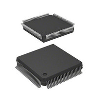
IC H8 MCU ROMLESS QFP112
Manufacturer
Renesas Electronics America
Series
H8® H8/300Hr
Datasheet
1.D13003TF16V.pdf
(717 pages)
Specifications of HD6413003TF16
Core Processor
H8/300H
Core Size
16-Bit
Speed
16MHz
Connectivity
SCI
Peripherals
DMA, PWM, WDT
Number Of I /o
50
Program Memory Type
ROMless
Ram Size
512 x 8
Voltage - Supply (vcc/vdd)
2.7 V ~ 5.5 V
Data Converters
A/D 8x10b
Oscillator Type
Internal
Operating Temperature
-20°C ~ 75°C
Package / Case
112-QFP
Lead Free Status / RoHS Status
Contains lead / RoHS non-compliant
Eeprom Size
-
Program Memory Size
-
Available stocks
Company
Part Number
Manufacturer
Quantity
Price
Company:

Part Number:
HD6413003TF16
Manufacturer:
Renesas Electronics America
Quantity:
10 000
Company:
Part Number:
HD6413003TF16V
Manufacturer:
ITT
Quantity:
12 000
Company:
Part Number:
HD6413003TF16V
Manufacturer:
RENESAS
Quantity:
36
Part Number:
HD6413003TF16V
Manufacturer:
RENESAS/瑞萨
Quantity:
20 000


11.4
Section 12
12.1
12.2
12.3
12.4
12.5
Section 13
13.1
13.2
11.3.2
11.3.3
11.3.4
11.3.5
Usage Notes .................................................................................................................... 405
11.4.1
11.4.2
Overview ........................................................................................................................ 407
12.1.1
12.1.2
12.1.3
12.1.4
Register Descriptions...................................................................................................... 410
12.2.1
12.2.2
12.2.3
12.2.4
Operation ........................................................................................................................ 417
12.3.1
12.3.2
12.3.3
12.3.4
Interrupts ........................................................................................................................ 421
Usage Notes .................................................................................................................... 421
Overview ........................................................................................................................ 423
13.1.1
13.1.2
13.1.3
13.1.4
Register Descriptions...................................................................................................... 427
13.2.1
13.2.2
13.2.3
13.2.4
13.2.5
13.2.6
13.2.7
Output Timing................................................................................................. 399
Normal TPC Output........................................................................................ 400
Non-Overlapping TPC Output........................................................................ 402
TPC Output Triggering by Input Capture....................................................... 404
Operation of TPC Output Pins........................................................................ 405
Note on Non-Overlapping Output .................................................................. 405
Features........................................................................................................... 407
Block Diagram................................................................................................ 408
Pin Configuration............................................................................................ 408
Register Configuration.................................................................................... 409
Timer Counter (TCNT)................................................................................... 410
Timer Control/Status Register (TCSR)........................................................... 411
Reset Control/Status Register (RSTCSR) ...................................................... 413
Notes on Register Access ............................................................................... 415
Watchdog Timer Operation............................................................................. 417
Interval Timer Operation ................................................................................ 418
Timing of Setting of Overflow Flag (OVF) .................................................... 419
Timing of Setting of Watchdog Timer Reset Bit (WRST) ............................. 420
Features........................................................................................................... 423
Block Diagram................................................................................................ 425
Input/Output Pins............................................................................................ 426
Register Configuration.................................................................................... 426
Receive Shift Register (RSR) ......................................................................... 427
Receive Data Register (RDR)......................................................................... 427
Transmit Shift Register (TSR) ........................................................................ 428
Transmit Data Register (TDR)........................................................................ 428
Serial Mode Register (SMR) .......................................................................... 429
Serial Control Register (SCR) ........................................................................ 433
Serial Status Register (SSR) ........................................................................... 437
Watchdog Timer
Serial Communication Interface
........................................................................................ 407
........................................................... 423
Related parts for HD6413003TF16
Image
Part Number
Description
Manufacturer
Datasheet
Request
R

Part Number:
Description:
KIT STARTER FOR M16C/29
Manufacturer:
Renesas Electronics America
Datasheet:

Part Number:
Description:
KIT STARTER FOR R8C/2D
Manufacturer:
Renesas Electronics America
Datasheet:

Part Number:
Description:
R0K33062P STARTER KIT
Manufacturer:
Renesas Electronics America
Datasheet:

Part Number:
Description:
KIT STARTER FOR R8C/23 E8A
Manufacturer:
Renesas Electronics America
Datasheet:

Part Number:
Description:
KIT STARTER FOR R8C/25
Manufacturer:
Renesas Electronics America
Datasheet:

Part Number:
Description:
KIT STARTER H8S2456 SHARPE DSPLY
Manufacturer:
Renesas Electronics America
Datasheet:

Part Number:
Description:
KIT STARTER FOR R8C38C
Manufacturer:
Renesas Electronics America
Datasheet:

Part Number:
Description:
KIT STARTER FOR R8C35C
Manufacturer:
Renesas Electronics America
Datasheet:

Part Number:
Description:
KIT STARTER FOR R8CL3AC+LCD APPS
Manufacturer:
Renesas Electronics America
Datasheet:
Part Number:
Description:
KIT STARTER FOR RX610
Manufacturer:
Renesas Electronics America
Datasheet:

Part Number:
Description:
KIT STARTER FOR R32C/118
Manufacturer:
Renesas Electronics America
Datasheet:

Part Number:
Description:
KIT DEV RSK-R8C/26-29
Manufacturer:
Renesas Electronics America
Datasheet:

Part Number:
Description:
KIT STARTER FOR SH7124
Manufacturer:
Renesas Electronics America
Datasheet:

Part Number:
Description:
KIT STARTER FOR H8SX/1622
Manufacturer:
Renesas Electronics America
Datasheet:

Part Number:
Description:
KIT DEV FOR SH7203
Manufacturer:
Renesas Electronics America
Datasheet: