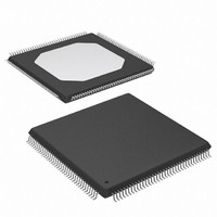
XC3S250E-4TQG144C Xilinx Inc, XC3S250E-4TQG144C Datasheet - Page 131

XC3S250E-4TQG144C
Manufacturer Part Number
XC3S250E-4TQG144C
Description
IC SPARTAN-3E FPGA 250K 144TQFP
Manufacturer
Xilinx Inc
Series
Spartan™-3Er
Datasheet
1.XC3S100E-4VQG100C.pdf
(233 pages)
Specifications of XC3S250E-4TQG144C
Number Of Logic Elements/cells
5508
Number Of Labs/clbs
612
Total Ram Bits
221184
Number Of I /o
108
Number Of Gates
250000
Voltage - Supply
1.14 V ~ 1.26 V
Mounting Type
Surface Mount
Operating Temperature
0°C ~ 85°C
Package / Case
144-LQFP
For Use With
813-1009 - MODULE USB-TO-FPGA TOOL W/MANUAL
Lead Free Status / RoHS Status
Lead free / RoHS Compliant
Other names
122-1524
Available stocks
Company
Part Number
Manufacturer
Quantity
Price
Company:
Part Number:
XC3S250E-4TQG144C
Manufacturer:
XILINX
Quantity:
2 000
Company:
Part Number:
XC3S250E-4TQG144C
Manufacturer:
XILINX
Quantity:
2 400
Company:
Part Number:
XC3S250E-4TQG144C
Manufacturer:
Xilinx Inc
Quantity:
10 000
Part Number:
XC3S250E-4TQG144C
Manufacturer:
XILINX/赛灵思
Quantity:
20 000
Part Number:
XC3S250E-4TQG144CS1
Manufacturer:
XILINX/赛灵思
Quantity:
20 000
Table 92: Timing for the IOB Output Path
DS312-3 (v3.8) August 26, 2009
Product Specification
Notes:
1.
2.
3.
Clock-to-Output Times
T
Propagation Times
T
T
Set/Reset Times
T
T
IOCKP
IOOP
IOOLP
IOSRP
IOGSRQ
Symbol
The numbers in this table are tested using the methodology presented in
Table 77
This time requires adjustment whenever a signal standard other than LVCMOS25 with 12 mA drive and Fast slew rate is assigned to the
data Output. When this is true, add the appropriate Output adjustment from
For minimum delays use the values reported by the Timing Analyzer.
R
and
Table
When reading from the Output Flip-Flop
(OFF), the time from the active transition
at the OCLK input to data appearing at
the Output pin
The time it takes for data to travel from
the IOB’s O input to the Output pin
The time it takes for data to travel from
the O input through the OFF latch to the
Output pin
Time from asserting the OFF’s SR input
to setting/resetting data at the Output
pin
Time from asserting the Global Set
Reset (GSR) input on the
STARTUP_SPARTAN3E primitive to
setting/resetting data at the Output pin
80.
Description
www.xilinx.com
LVCMOS25
output drive, Fast slew
rate
LVCMOS25
output drive, Fast slew
rate
LVCMOS25
output drive, Fast slew
rate
Conditions
Table 95
Table
(2)
(2)
(2)
94.
, 12 mA
, 12 mA
, 12 mA
and are based on the operating conditions set forth in
DC and Switching Characteristics
Device
All
All
All
Speed Grade
Max
2.18
2.24
2.32
3.27
8.40
-5
Max
2.50
2.58
2.67
3.76
9.65
-4
Units
ns
ns
ns
ns
ns
131


