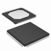
XC3S250E-4TQG144C Xilinx Inc, XC3S250E-4TQG144C Datasheet - Page 50

XC3S250E-4TQG144C
Manufacturer Part Number
XC3S250E-4TQG144C
Description
IC SPARTAN-3E FPGA 250K 144TQFP
Manufacturer
Xilinx Inc
Series
Spartan™-3Er
Datasheet
1.XC3S100E-4VQG100C.pdf
(233 pages)
Specifications of XC3S250E-4TQG144C
Number Of Logic Elements/cells
5508
Number Of Labs/clbs
612
Total Ram Bits
221184
Number Of I /o
108
Number Of Gates
250000
Voltage - Supply
1.14 V ~ 1.26 V
Mounting Type
Surface Mount
Operating Temperature
0°C ~ 85°C
Package / Case
144-LQFP
For Use With
813-1009 - MODULE USB-TO-FPGA TOOL W/MANUAL
Lead Free Status / RoHS Status
Lead free / RoHS Compliant
Other names
122-1524
Available stocks
Company
Part Number
Manufacturer
Quantity
Price
Company:
Part Number:
XC3S250E-4TQG144C
Manufacturer:
XILINX
Quantity:
2 000
Company:
Part Number:
XC3S250E-4TQG144C
Manufacturer:
XILINX
Quantity:
2 400
Company:
Part Number:
XC3S250E-4TQG144C
Manufacturer:
Xilinx Inc
Quantity:
10 000
Part Number:
XC3S250E-4TQG144C
Manufacturer:
XILINX/赛灵思
Quantity:
20 000
Part Number:
XC3S250E-4TQG144CS1
Manufacturer:
XILINX/赛灵思
Quantity:
20 000
Functional Description
clock distribution network, the clock signal returns to the
DLL via a feedback line called CLKFB. The control block
inside the DLL measures the phase error between CLKFB
and CLKIN. This phase error is a measure of the clock skew
that the clock distribution network introduces. The control
block activates the appropriate number of delay steps to
cancel out the clock skew. When the DLL phase-aligns the
Table 29: DLL Attributes
DLL Clock Input Connections
For best results, an external clock source enters the FPGA
via a Global Clock Input (GCLK). Each specific DCM has
four possible direct, optimal GCLK inputs that feed the
DCM’s CLKIN input, as shown in
provides the specific pin numbers by package for each
GCLK input. The two additional DCM’s on the XC3S1200E
and XC3S1600E have similar optimal connections from the
left-edge LHCLK and the right-edge RHCLK inputs, as
described in
50
CLK_FEEDBACK
CLKIN_DIVIDE_BY_2
CLKDV_DIVIDE
CLKIN_PERIOD
Attribute
Table 31
and
Table
32.
Table
Chooses either the CLK0 or CLK2X output to
drive the CLKFB input
Halves the frequency of the CLKIN signal just
as it enters the DCM
Selects the constant used to divide the CLKIN
input frequency to generate the CLKDV
output frequency
Additional information that allows the DLL to
operate with the most efficient lock time and
the best jitter tolerance
30.
Table 30
Description
www.xilinx.com
also
CLK0 signal with the CLKIN signal, it asserts the LOCKED
output, indicating a lock on to the CLKIN signal.
DLL Attributes and Related Functions
The DLL unit has a variety of associated attributes as
described in
the sections that follow.
•
Design Note
Avoid using global clock input GCLK1 as it is always shared
with the M2 mode select pin. Global clock inputs GCLK0,
GCLK2, GCLK3, GCLK12, GCLK13, GCLK14, and
GCLK15 have shared functionality in some configuration
The DCM supports differential clock inputs (for
example, LVDS, LVPECL_25) via a pair of GCLK inputs
that feed an internal single-ended signal to the DCM’s
CLKIN input.
Table
29. Each attribute is described in detail in
NONE, 1X, 2X
FALSE, TRUE
1.5, 2, 2.5, 3, 3.5, 4, 4.5, 5, 5.5, 6.0,
6.5, 7.0, 7.5, 8, 9, 10, 11, 12, 13, 14,
15, and 16
Floating-point value representing the
CLKIN period in nanoseconds
DS312-2 (v3.8) August 26, 2009
Values
Product Specification
R


